www.ti.com
4
Power Supplies
5
Using the EVM
5.1
Development/Evaluation Board
5.1.1
EVM and TSW1100 Capture Board
Power Supplies
The ADS1610EVM arrives with CS, HOST_RD, HOST_A2, and HOST_A3 signals set LOW. This enables
the ADS1610 and at power up allows the device to start converting. The modes pins (M0 and M1) are
factory set to enable a data rate of 10 MHz.
The ADS1610EVM board requires various power sources for operation.
•
A dual
±
7-Vdc supply for best performance of the analog front end and reference generation circuitry.
These voltages can be applied at J11.
•
Two +5-Vdc supplies for the ADS1610 analog supply and clock supply. Apply 5 V at J12 and J13.
•
A 3-Vdc supply for digital section of the board (A/D + address d buffers). Apply 3 V to
J1.
The ADS1610EVM serves two purposes. It functions as an evaluation/development board and a reference
design.
The two common methods used to evaluate the ADS1610EVM’s performance are:
1. EVM used as a stand-alone system. The user is responsible for capturing and analyzing the data,
typically via a logic analyzer and analysis software (LABView, MATLAB, etc.).
2. EVM used with TI’s TSW1100 data capture board solution:
http://focus.ti.com/docs/toolsw/folders/print/tsw1100.html
The user’s guide for the data capture board (
) provides detailed information and setup
instructions.
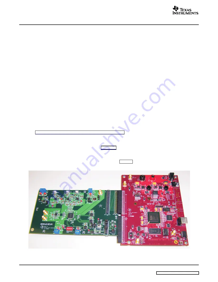
The ADS1610EVM mates with the TSW1100 board via J2. Two data ports are available on the data
capture board; the reference designators are J1 and J2.
shows the ADS1610 plugged into the
TSW1100 board.
Figure 2. TSW1100 and ADS1610EVM Setup
8
ADS1610EVM
SLAU180A – May 2006 – Revised August 2006


