background image

GND

5 to 36 V

Amp VCC+

J10

J13

J11

J12

JP17
open

TPS5420D

Switching Regulator to 5.3V

TPS7A4501

LDO Regulator to 5V

J

P

1

6

1

J

P

1

9

1

TPS79633

LDO 3.3V

TPS79601

LDO 1.8V

(option for 3.3V)

5 V

Analog

VDD

Digital

VDD

THS4509

TPS79601

LDO 3.3V

TPS79633

LDO 3.3V

To Clock Gen

option, to USB

port

To ADC

To ADC

To Clock

Generator

Option

To Clock

Generator

Option, USB

Port, CMOS

buffer

To USB

Port

Amp VCC-

PWR IN

J17

Circuit Description

www.ti.com

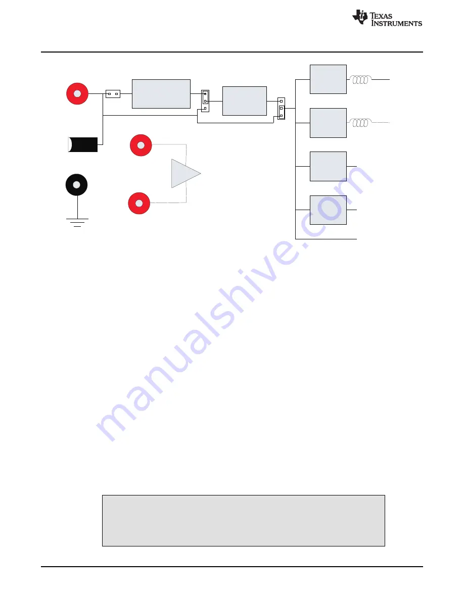
Figure 2. ADS62PXXEVM Power Distribution

2.2.2

EVM Power Connections

Power is supplied to the EVM through banana jacks. From this input power, several different ways of
delivering power to the ADC and other EVM functions are available.

Figure 2

shows a simplified

representation of the power options available for the ADS62PXXEVM. The default option is to provide 5V
to J10 or J17, and from there, the EVM generates 3.3V for the analog supply to the ADC and the
necessary digital supply voltage for the populated ADC. The EVM also generates the proper voltages for
optional features of the EVM such as the Clock Generation circuitry, the USB circuitry, and the CMOS
output buffer.

Some ADC devices that may be evaluated on the ADS62PXXEVM platform do not take 1.8V for the digital
supply, but rather require 3.3V for the digital supply. For this reason, an adjustable voltage regulator was
chosen for the digital supply; the output may be changed to 3.3V by changing the value of a resistor, R269
and capacitor C148. The resistor and capacitor need not to be changed in the field unless the ADC is
being changed, because the EVM ships with the correct digital supply voltage for the ADC that is installed.
For reference, ADS62P42/43/44/45,ADS62P22/23/24/25 and ADS62C15 use 3.3V as digital supply for the
ADC whereas ADS62P48/49,ADS62P28/29 and ADS62C17 use 1.8V as digital supply for the ADC.

Power for the optional THS4509 operational amplifier is supplied by banana jacks J11 and J13. If the
amplifier is being evaluated in AC coupled configuration, 5V is supplied to J11, and J13 is connected to
ground. In DC-coupled configuration, 4V is supplied to J11 and –1V is supplied to J13. Otherwise, these
inputs may be left unconnected.

Although various power options are available on this EVM, care must be taken while applying power on
J10 or J17 as different options have different voltage ranges specified.

Table 2

displays the general

jumper setting information;

Table 3

displays the various power option settings. Prior to making any jumper

settings, see the schematics located in the design package.

CAUTION

Voltage limits: Exceeding the maximum input voltages can damage EVM
components. Undervoltage can cause improper operation of some or all of the
EVM components.

8

ADS62PXXEVM

SLAU237B – May 2008 – Revised July 2010

Copyright © 2008–2010, Texas Instruments Incorporated

Summary of Contents for ADS62PXXEVM

Page 1: ...ADS62PXXEVM User s Guide Literature Number SLAU237B May 2008 Revised July 2010 ...

Page 2: ...2 SLAU237B May 2008 Revised July 2010 Copyright 2008 2010 Texas Instruments Incorporated ...

Page 3: ...SPI Control Software 15 3 2 Setting Up the EVM for ADC SPI Control 16 3 3 Using the TI ADC SPI Interface Software 17 4 Connecting to FPGA Platforms 19 4 1 TSW1200 Capture Board 19 4 2 TSW1100 22 5 ADC Evaluation 23 5 1 Hardware Selection 23 5 2 Coherent Input Frequency Selection 24 6 Revision Changes 24 3 SLAU237B May 2008 Revised July 2010 Table of Contents Copyright 2008 2010 Texas Instruments I...

Page 4: ...ough Onboard VCXO CDCE72010 and Crystal Filter 21 11 ADC Performance With Clock Through Onboard VCXO CDCE72010 Configured for Differential LVPECL Output 22 List of Tables 1 Jumper List 6 2 EVM Power Supply Jumper Description 9 3 EVM Power Supply Options 9 4 Analog Input Jumper description 10 5 EVM Analog Input Options 11 6 Clock Input Jumper Description 12 7 EVM Clock Input Options 13 8 ADS62PXX F...

Page 5: ... ADS62P42 43 44 45 48 49 ADS62P22 23 24 25 28 29 and ADS62C15 17 analog to digital converters ADC which will be collectively referred to as ADS62PXX This document should be used in combination with respective ADC data sheet The ADS62PXX EVM provides a platform for evaluating the analog to digital converter ADC under various signal clock reference and power supply conditions 1 1 EVM Block Diagram P...

Page 6: ...0 to J10 on the ADC EVM Do not connect a voltage source greater than 5 5V 3 Switch on power supplies 4 Using a function generator with 50Ω output impedance generate a 0V offset 1 5VPP sine wave clock into J19 The frequency of the clock must be within the specification for the device speed grade 5 Use a frequency generator with a 50Ω output impedance generate a 0V offset 1 dBFS amplitude sine wave ...

Page 7: ...ADC Circuit Function Selection of various modes of operation of the ADS62PXX EVM is most often controlled by jumpers on the EVM either by placing shunts on 0 025 inch square jumper posts or by installation of surface mount 0Ω resistors In general the use of 0Ω resistors as jumpers are used in the clock or signal path where signal integrity is critical and jumper posts are used for static or low sp...

Page 8: ...ble voltage regulator was chosen for the digital supply the output may be changed to 3 3V by changing the value of a resistor R269 and capacitor C148 The resistor and capacitor need not to be changed in the field unless the ADC is being changed because the EVM ships with the correct digital supply voltage for the ADC that is installed For reference ADS62P42 43 44 45 ADS62P22 23 24 25 and ADS62C15 ...

Page 9: ...ing this option take care powering up the EVM because higher voltage or reverse polarity can damage it This is the default power supply configuration for the ADS62PXXEVM 2 2 2 2 Power Supply Option 2 Option 2 supplies the power to the ADC using cascaded topology of the TPS5420D switching power regulator and the TPS7A4501 Low Drop Out regulator The TPS5420 is a step down converter which works with ...

Page 10: ...f these options the EVM must be configured for one of the options listed in Table 5 See the schematic located in the design package prior to making any jumper changes Table 4 Analog Input Jumper description EVM Jumper Description Jumper Setting J6 Analog Input single ended J3 Analog Input single ended Analog input can be used with J6 for J7 Not populated differential input Analog input can be used...

Page 11: ...the ADC TI has a range of wideband operational amplifiers such as THS4508 09 11 13 20 On this EVM THS4509 is used as an example to amplify the input from J3 or J9 The THS4509 is powered up by applying 5 V to J11 and GND to J13 for AC coupled configuration A differential power supply 4V applied to J11 and 1V applied to J13 may also be used to power up the amplifier if common mode biasing is an issu...

Page 12: ...ter For better performance selecting the CMOS clock through a crystal output is recommended Prior to making any jumper settings see the schematic in the design package Table 6 displays the various clock option settings The VCXO and crystal filter do not come populated on the EVM by default although the CDCE72010 Clock buffer is installed Table 6 Clock Input Jumper Description EVM Jumper Descriptio...

Page 13: ...n J19 is stepped up by a factor of 2 ADC performance in this case depends on the clock source quality This option is also the default configuration on the EVM when it is shipped from the factory The test result using this option is shown in Figure 9 2 2 4 2 Clock Option 2 Option 2 uses the onboard VCXO and CDCE72010 to provide a clock to the ADC The CDCE72010 is used in SPI mode which uses the int...

Page 14: ...SW1200 will automatically terminate the LVDS outputs once the TSW1200 is connected to J8 The ADS62PXX and most other ADCs that may be evaluated on this EVM also have an option to output the digitized parallel data in the form of single ended CMOS If single ended CMOS is desired header post connectors J1 and J2 are provided for the CMOS output In order to use the header J1 a CMOS buffer U12 must be...

Page 15: ...nicate to the USB port that resides on the EVM When prompted users should allow the Windows operating system to search for device drivers by checking Yes this time only as seen in Figure 4 It will find the TI ADC SPI interface drivers automatically After the software is installed insert the USB cable to the EVM to finish the installation The Found New Hardware wizard will start and you must acknow...

Page 16: ...tion users must move several jumpers Move jumper JP11 to short positions 2 3 which places the ADC into serial operation mode Move jumper JP8 to short positions 2 3 which allows the USB circuit to control SCLK Move jumper JP9 to short positions 2 3 which allows the USB circuit to control SDATA Move jumper JP10 to short positions 2 3 which allows the USB circuit to control SEN 16 ADS62PXXEVM SLAU237...

Page 17: ...This can easily be done by pressing the ADS62PXX Reset button found on the ADS62PXX tab For most ADS62PXX evaluations that make use of the SPI interface users should also assert the Override Bit also found on the ADS62PXX tab This will force the ADC to be configured by the SPI interface only and it will ignore any board level settings that may have been set Please consult the datasheet for a full ...

Page 18: ...h configures the ADC for use with the TSW1200 When ready to write the contents of the script file to the ADC users can press the Load Script button and they will be prompted for the file location of their script file The commands are sent to the ADC when the user acknowledges the selection of the file however the graph indicator does not show multiple writes The ADC SPI History will update to show...

Page 19: ...o start the TSW1200 software note the following points Users should consult the TSW1200 documentation for configuration details Figure 8 TSW1200 GUI Introduction 1 Select the ADC type to be used before capturing 2 For test select Single Tone FFT plot 3 For the ADC Sampling Rate type in the value 4 Type in the ADC Input Frequency Auto calculation of the input frequency depends on the FFT record len...

Page 20: ...r J3 Channel B to the ADC This setup uses Power Option 1 Table 3 Analog Input Option 1 Table 5 and Clock Option 1 Table 7 which is the default on the EVM Figure 9 shows the ADC performance capture using TSW1200 with the input signal of a 57 6 MHz frequency and clock frequency of 250 MHz with ADS62PXX Figure 9 Quick Setup Test Result 20 ADS62PXXEVM SLAU237B May 2008 Revised July 2010 Copyright 2008...

Page 21: ...e ADC The CDCE72010 provides a single ended clock through output Y0 Table 7 which is passed through a crystal filter of center frequency 245 76 MHz This was the example setup the VCXO and the crystal filter are not populated on the EVM because the values depend on the end application sampling rate The capture result for ADS62PXX is as shown in Figure 10 Figure 10 ADC Performance With Clock Through...

Page 22: ...With Clock Through Onboard VCXO CDCE72010 Configured for Differential LVPECL Output 4 2 TSW1100 When the ADS62PXX is configured in CMOS output mode users can use TI s TSW1100 capture board Several additional board configuration steps are required before using this option Remove resistor packs with the following reference designators RN7 RN8 RN9 RN10 RN11 RN12 RN13 and RN14 Install TI s SN74AVC1624...

Page 23: ...the ADC digitizes the performance of the source Noise can be broken into two components broadband noise and close in phase noise Broadband noise can be improved by adding an LC filter to improve distortion performance however the close in phase noise typically cannot be improved by additional filtering Therefore when selecting an analog signal source it is important to review the manufacturer s ph...

Page 24: ...d to as the fundamental frequency ff Determining the ADC input frequency is a two step process First select the frequency of interest for evaluating the ADC then divide this by the fundamental frequency This typically yields a non integer value which should be rounded to the nearest odd preferably prime integer Once that integer or frequency bin fbin has been determined multiply this with the fund...

Page 25: ...t This notice contains important safety information about temperatures and voltages For additional information on TI s environmental and or safety programs please contact the TI application engineer or visit www ti com esh No license is granted under any patent right or other intellectual property right of TI covering or relating to any machine process or combination in which such TI products or s...

Page 26: ...ch statements TI products are not authorized for use in safety critical applications such as life support where a failure of the TI product would reasonably be expected to cause severe personal injury or death unless officers of the parties have executed an agreement specifically governing such use Buyers represent that they have all necessary expertise in the safety and regulatory ramifications o...

Page 27: ...андарту ISO 9001 Лицензия ФСБ на осуществление работ с использованием сведений составляющих государственную тайну Поставка специализированных компонентов Xilinx Altera Analog Devices Intersil Interpoint Microsemi Aeroflex Peregrine Syfer Eurofarad Texas Instrument Miteq Cobham E2V MA COM Hittite Mini Circuits General Dynamics и др Помимо этого одним из направлений компании ЭлектроПласт является на...

Reviews: