Reference
2-3
Analog Interface
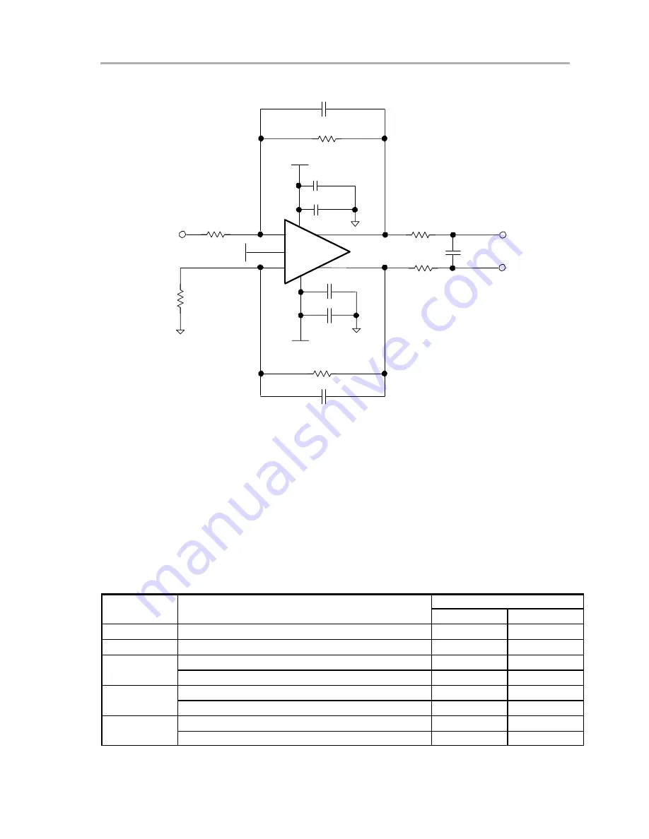
Figure 2 - 1. Input Buffer Circuit
1 k
Ω
1 k
Ω
+V
CC
V
I
0.1
µ
F
1
µ
F
25
Ω
(+) IN
( - ) IN
6800 pF
1
µ
F
0.1
µ
F
1 k
Ω
- V
CC
-
+
60 pF
1 k
Ω
60 pF
V
OCM
25
Ω
-
+
THS4503
+2.048 V
2.2
Reference
The EVM allows users to select from three reference sources. The
ADS8402/ADS8412EVM provides an onboard 4.096-V reference, U3. The
EVM also has the provision for users to supply a reference voltage via
connecter P1 pin 20. The user reference voltage and onboard reference
voltages can be filtered by installing amplifier U1. Both the ADS8402 and
ADS8412 analog-to-digital converters have integrated onboard reference
buffers; therefore, it is not necessary to buffer the voltage externally. The
reference buffer circuit on the EVM is not populated with an amplifier. The EVM
comes installed with an on-chip internal reference tied directly to the reference
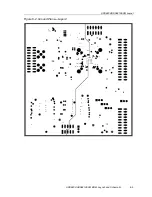
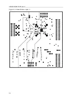
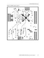
pin of the converter. See Chapter 6 for the schematic.
Table 2 - 2. Solder Short Jumper Setting
Reference
Description
Jumper Setting
Reference
Designator
Description
1 - 2
2 - 3
SJP1
Not used on the EVM
SJP2
On-chip internal reference applied to reference pin
Installed
†
SJP3
Apply reference voltage from external source
Not Installed
Installed
Apply voltage to amplifier, U2, common-mode voltage pin
Installed
†
N/A
SJP4
Buffer onboard reference, REF3040
Installed
Not installed
Buffer user reference voltage applied at P1 pin 20.
Not Installed
Installed
SJP5
Select REF3040 for reference voltage
Installed
Not installed
Select buffered reference voltage
Not Installed
Installed
†
Factory set condition


