background image

V

OUT

 x (V

IN

 - V

OUT

)

I

LR

 x f

SW 

x V

IN

L =

R1 

t

1.3 x 10

-10

V

IN(MAX)

 x 150 ns

V

OUT

1.3 x 10

-10

 x f

SW

R1 =

R3 = 2.21 k

:

- 1

V

OUT

0.8

= 6.91 k

:

=

V

OUT

0.8

R3

R4

- 1

www.ti.com

Design Procedure

Step 1: Calculate the feedback resistors

The ratio of the feedback resistors can be calculated from the following equation:

(1)

As a general practice, R3 and R4 should be chosen from standard 1% resistor values in the range of
1.0 k

to 10 k

satisfying the above ratio. Now, select R4 = 2.21 k

, with V

OUT

= 3.3V,

(2)

Step 2: Calculate the on-time setting resistor

The switching frequency f

SW

of the demonstration board is affected by the on-time t

on

of the LM3102, which

is determined by R1. If f

SW

and V

OUT

are determined, R1 can be calculated as follows:

(3)

For this demonstration board design, V

OUT

= 3.3V and f

SW

= 500 kHz are chosen. As a result,

R1 = 50.8 k

. To ensure that the on-time is larger than the minimum limit, which is 150 ns, the value of

R1 must satisfy the following equation:

(4)

Now the maximum V

IN

is 42V, the calculated R1 satisfies

Equation 4

.

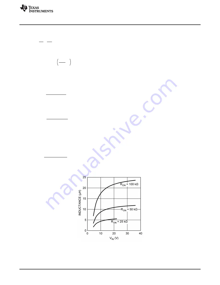
Step 3: Determine the inductance

The main parameter affected by the inductor is the amplitude of the inductor current ripple I

LR

. Once I

LR

is

selected, L can be determined by:

(5)

For this demonstration board design, I

LR

= 0.5A is selected. Now V

IN

= 18V, V

OUT

= 3.3V, and

f

SW

= 500 kHz. As a result, L = 10.78 µH.

Figure 2. Inductor Selection for V

OUT

= 3.3V

3

SNVA248 – October 2007

AN-1646 LM3102 Demonstration Board Reference Design

Submit Documentation Feedback

Copyright © 2007, Texas Instruments Incorporated

Summary of Contents for AN-1646

Page 1: ...line variations due to the inverse relationship between the input voltage and the on time Protection features include output over voltage protection thermal shutdown VCC under voltage lock out gate drive under voltage lock out The LM3102 is available in the thermally enhanced eTSSOP 20 package This user s guide details the design of a demonstration board which provides a 3 3V output voltage with 2...

Page 2: ... Typ Max Unit Input Voltage VIN 8 18 42 V Output Voltage VOUT 3 2 3 3 3 4 V Output Current IOUT 0 2 5 A Output Voltage Ripple VOUT Ripple 50 mVp p Output Voltage Regulation ΔVOUT ALL VIN and IOUT Conditions 3 3 Efficiency VIN 8V 84 92 VIN 24V 73 85 VIN 42V 62 79 IOUT 0 1A to 2 5A Output Short Current Limit ILIM SC 2 95 A 5 Design Procedure The LM3102 is easy to use compared with other devices avai...

Page 3: ... If fSW and VOUT are determined R1 can be calculated as follows 3 For this demonstration board design VOUT 3 3V and fSW 500 kHz are chosen As a result R1 50 8 kΩ To ensure that the on time is larger than the minimum limit which is 150 ns the value of R1 must satisfy the following equation 4 Now the maximum VIN is 42V the calculated R1 satisfies Equation 4 Step 3 Determine the inductance The main p...

Page 4: ...ge the main MOSFET gate driver at turn on Low ESR also helps ensure a complete recharge during each off time C5 The capacitor at the SS pin determines the soft start time that is the time for the reference voltage at the regulation comparator and the output voltage to reach their final value The time is determined from the following equation 7 In this demonstration board a 10 nF capacitor is used ...

Page 5: ...ND pin pin 7 The output capacitor C10 C11 should be connected close to the load and tied directly to the ground plane The inductor L1 should be connected close to the SW pin with as short a trace as possible to reduce the potential for EMI electromagnetic interference generation If it is expected that the internal dissipation of the LM3102 will produce excessive junction temperature during normal ...

Page 6: ...3102 Demonstration Board PCB Top View Figure 5 LM3102 Demonstration Board PCB Bottom View 6 AN 1646 LM3102 Demonstration Board Reference Design SNVA248 October 2007 Submit Documentation Feedback Copyright 2007 Texas Instruments Incorporated ...

Page 7: ...10 ECJ4YB0J476M Panasonic C12 0603 X7R 0 1µF 25V 0603 GRM188R71E104KA01B muRata R1 Resistor Chip 51 1kΩ F 0603 CRCW06035112F Vishay R3 Resistor Chip 6 81kΩ F 0603 CRCW06036811F Vishay R4 Resistor Chip 2 21kΩ F 0603 CRCW06032211F Vishay L1 Inductor 10µH 4 40A POWER CHOKE 10 3 10 5 4 CDRH104RNP 100NC Sumida SMD Power Choke WE TPC 3 6A Type XLH 10 10 3 8 744066100 Wurth U1 IC LM3102 eTSSOP 20 LM3102M...

Page 8: ...A 25 C unless otherwise specified Efficiency vs Load Current VOUT Regulation vs Load Current VOUT 3 3V VOUT 3 3V Continuous Mode Operation Discontinuous Mode Operation VOUT 3 3V 2 5A Loaded VOUT 3 3V 0 1A Loaded 8 AN 1646 LM3102 Demonstration Board Reference Design SNVA248 October 2007 Submit Documentation Feedback Copyright 2007 Texas Instruments Incorporated ...

Page 9: ...OUT 3 3V 0 1A 2 5A Load Current slew rate 2 5A µs Power Up Enable Transient VOUT 3 3V 2 5A Loaded VOUT 3 3V 2 5A Loaded Shutdown Transient VOUT 3 3V 2 5A Loaded 9 SNVA248 October 2007 AN 1646 LM3102 Demonstration Board Reference Design Submit Documentation Feedback Copyright 2007 Texas Instruments Incorporated ...

Page 10: ...esponsible for compliance with all legal regulatory and safety related requirements concerning its products and any use of TI components in its applications notwithstanding any applications related information or support that may be provided by TI Buyer represents and agrees that it has all the necessary expertise to create and implement safeguards which anticipate dangerous consequences of failur...

Reviews: