Layout and Bill of Material
7
Layout and Bill of Material
7.1
Layout
7.1.1
Printed-Circuit Board Layout Guideline
The primary concerns when laying out a custom receiver PCB are:
•
AC1 and AC2 trace resistance
•
OUT trace resistance
•
RECT trace resistance
•
GND connection
•
Copper weight
≥
2 oz
For a 720-mA load current application, the current rating for each net is as follows:
•
AC1 = AC2 = 900 mA
•
BOOT1 = BOOT2 = 10 mA
•
RECT = 750 mA
•
OUT = 750 mA
•
COM1 = COM2 = 300 mA
•
CLAMP1 = CLAMP2 = 500 mA
•
ILIM = 10 mA
•
AD = AD_EN = TS-CTRL = EN1 = EN2 = TERM = FOD = 1 mA
•
CHG = 10 mA
It is also recommended to have the following capacitance on RECT and OUT:
•
RECT
≥
±10
μ
F
•
OUT
≥
1
μ
F
It is always a good practice to place high-frequency bypass capacitors of 0.1
μ
F next to RECT and OUT.
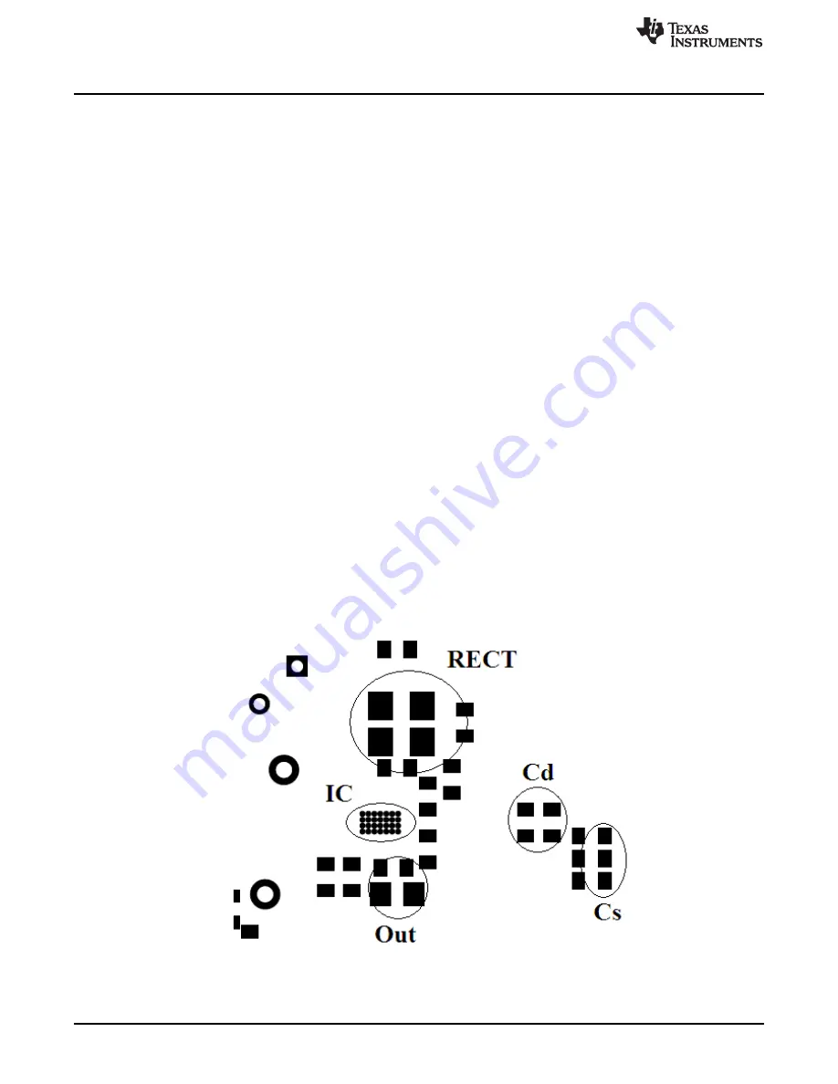
illustrates an example of a WCSP layout:
Figure 8. bq51010BEVM-764 Layout Example
14
bq51010BEVM-764 Evaluation Module (WCSP Package)
SLUUAE3A – August 2013 – Revised December 2013
Copyright © 2013, Texas Instruments Incorporated


