6.15 Timing Requirements: GPIO
all input signals are specified with t
r
= t
f
= 1 V/ns (10% to 90% of V
IO
) and timed from a voltage level of (VIL + VIH) / 2,
1.7 V ≤ V
IO
≤ 5.5 V, 1.7 V ≤ V
DD
≤ 5.5 V, and –40°C ≤ T
A
≤ +125°C
MIN
NOM
MAX
UNIT
t
GPIHIGH
GPI high time
2
µs
t
GPILOW
2
µs
t
GPAWGD
LDAC falling edge to DAC update delay
2
µs
t
CS2LDAC
SYNC rising edge to LDAC falling edge
1
µs
t
STP2LDAC
I
2
C stop bit rising edge to LDAC falling edge
1
µs
t
LDACW
LDAC low time
2
µs
(1)
The SCL, SDA, A0, and A1 pins can be configured as GPIOs that perform different channel-specific or independent operations. The
actual response time of the GPIO is determined by the delay provided by the configured function and the settling time of the DAC.
(2)
The GPIOs can be configured as channel-specific or global LDAC function.
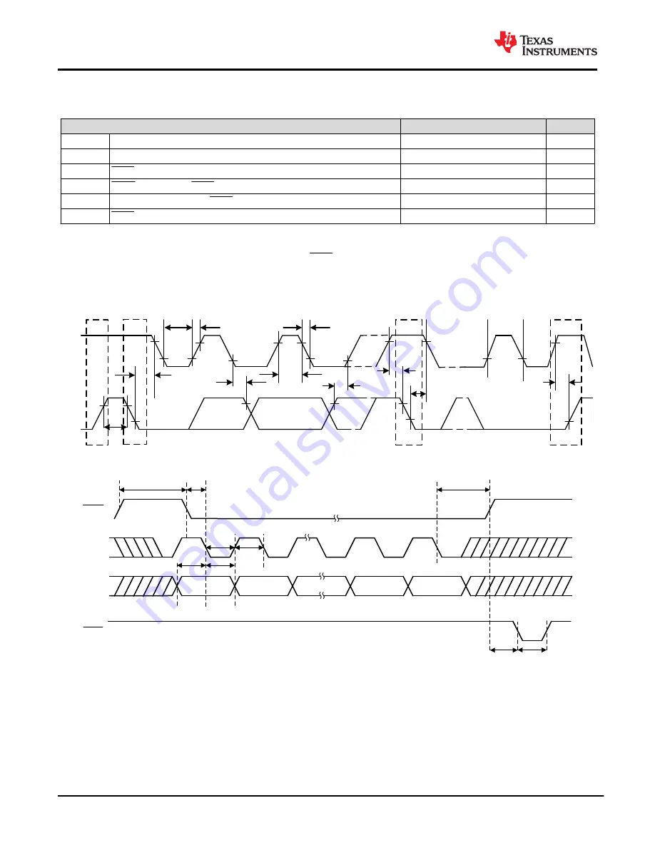
6.16 Timing Diagrams
SCL
SDA
P
S
t
BUF
t
HDSTA
t
LOW
t
R
t
HDDAT
t
HIGH
t
F
t
SUDAT
t
SUSTA
t
HDSTA
S
t
SUSTO
P
Low byte ACK cycle
Figure 6-1. I
2
C Timing Diagram
t
CSS
t
SDIS
t
SDIH
SYNC
SDI
t
CSHIGH
Bit 23
t
SCLKLOW
Bit 1
Bit 0
t
CSH
SCLK
t
SCLKHIGH
t
CS2LDAC
t
LDACW
GPIO/
LDAC
Figure 6-2. SPI Write Timing Diagram
DAC53001, DAC53002, DAC63001, DAC63002
SLASF48 – MAY 2022
12
Copyright © 2022 Texas Instruments Incorporated
Product Folder Links:


