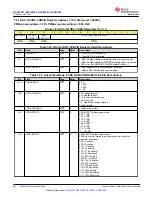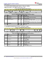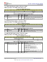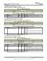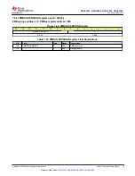
7.6.4 DAC-X-VOUT-CMP-CONFIG Register (address = 15h, 03h) [reset = 0000h]
PMBus page address = FFh, PMBus register address = DDh, D1h
Figure 7-25. DAC-X-VOUT-CMP-CONFIG Register (X = 0, 1)
15
14
13
12
11
10
9
8
7
6
5
4
3
2
1
0
X
VOUT-GAIN-X
X
CMP-
X-OD-
EN
CMP-
X-OUT-
EN
CMP-X-
HIZ-IN-
DIS
CMP-
X-INV-
EN
CMP-
X-EN
X-0h
R/W-0h
X-0h
R/W-0h R/W-0h
R/W-0h
R/W-0h R/W-0h
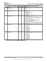
Table 7-26. DAC-X-VOUT-CMP-CONFIG Register Field Descriptions
Bit
Field
Type
Reset
Description
15-13
X
X
0h
Don't care
12-10
VOUT-GAIN-X
R/W
0h
000: Gain = 1x, external reference on VREF pin
001: Gain = 1x, VDD as reference
010: Gain = 1.5x, internal reference
011: Gain = 2x, internal reference
100: Gain = 3x, internal reference
101: Gain = 4x, internal reference
Others: Invalid
9-5
X
X
0h
Don't care
4
CMP-X-OD-EN
R/W
0
0: Set OUTx pin as push-pull
1: Set OUTx pin as open-drain in comparator mode (CMP-X-EN =
1 and CMP-X-OUT-EN = 1)
3
CMP-X-OUT-EN
R/W
0
0: Generate comparator output but consume internally
1: Bring comparator output to the respective OUTx pin
2
CMP-X-HIZ-IN-DIS
R/W
0
0: FBx input has high-impedance. Input voltage range is limited.
1: FBx input is connected to resistor divider and has finite
impedance. Input voltage range is same as full-scale.
1
CMP-X-INV-EN
R/W
0
0: Don't invert the comparator output
1: Invert the comparator output
0
CMP-X-EN
R/W
0
0: Disable comparator mode
1: Enable comparator mode. Current-output must be in power-
down. Voltage-output mode must be enabled.
DAC53001, DAC53002, DAC63001, DAC63002
SLASF48 – MAY 2022
58
Copyright © 2022 Texas Instruments Incorporated
Product Folder Links:


