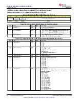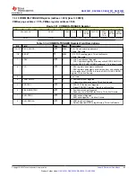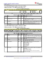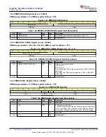
7.6.13 CMP-STATUS Register (address = 23h) [reset = 0000h]
PMBus page address = FFh, PMBus register address = E7h
Figure 7-34. CMP-STATUS Register
15
14
13
12
11
10
9
8
7
6
5
4
3
2
1
0
X
PROTECT-
FLAG
WIN-
CMP-0
X
WIN-
CMP-1
CMP-
FLAG-
0
X
CMP-
FLAG-
1
X-0h
R-0h
R-0h
X-0h
R-0h
R-0h
X-0h
R-0h
Table 7-37. CMP-STATUS Register Field Descriptions
Bit
Field
Type
Reset
Description
15-9, 6-5,
2-1
X
X
0
Don't care
8
PROTECT-FLAG
R
0
0: PROTECT operation not triggered.
1: PROTECT function is completed or in progress. This bit resets
to 0 when read.
7, 4
WIN-CMP-X
R
0
Window comparator output from respective channels. The output
is latched or unlatched based on the WINDOW-LATCH-EN
setting in the COMMON-CONFIG register.
3, 0
CMP-FLAG-X
R
0
Synchronized comparator output from respective channels.
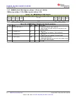
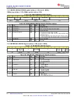
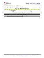
7.6.14 GPIO-CONFIG Register (address = 24h) [reset = 0000h]
PMBus page address = FFh, PMBus register address = E8h
Figure 7-35. GPIO-CONFIG Register
15
14
13
12
11
10
9
8
7
6
5
4
3
2
1
0
GF-EN
X
GPO-EN
GPO-CONFIG
GPI-CH-SEL
GPI-CONFIG
GPI-EN
R/W-0h
X-0h
R/W-0h
R/W-0h
R/W-0h
R/W-0h
R/W-0h
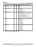
Table 7-38. GPIO-CONFIG Register Field Descriptions
Bit
Field
Type
Reset
Description
15
GF-EN
R/W
0
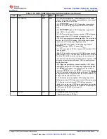
0: Glitch filter disabled for GP input. This setting provides faster
response.
1: Glitch filter enabled for GPI. This setting introduces additional
propagation delay but provides robustness.
14
X
X
0
Don't care.
13
GPO-EN
R/W
0
0: Disable output mode for GPIO pin.
1: Enable output mode for GPIO pin.
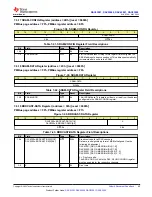
12-9
GPO-CONFIG
R/W
0000
STATUS function setting. The GPIO pin is mapped to the
following register bits as output:
0001: NVM-BUSY
0100: DAC-1-BUSY
0111: DAC-0-BUSY
1000: WIN-CMP-1
1011:WIN-CMP-0
Others: NA
8-5
GPI-CH-SEL
R/W
0000
Two bits correspond to two DAC channels. 0b is
disabled
and 1b
is
enabled
.
GPI-CH-SEL[0]: Channel 1
GPI-CH-SEL[3]: Channel 0
Example: when GPI-CH-SEL is 1001, both channel-0 and
channel-1 are enabled.
DAC53001, DAC53002, DAC63001, DAC63002
SLASF48 – MAY 2022
66
Copyright © 2022 Texas Instruments Incorporated
Product Folder Links:


