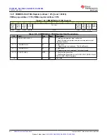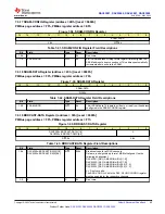
7.6.17 SRAM-CONFIG Register (address = 2Bh) [reset = 0000h]
PMBus page address = FFh, PMBus register address = EFh
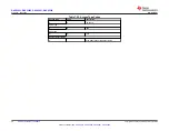
Figure 7-38. SRAM-CONFIG Register
15
14
13
12
11
10
9
8
7
6
5
4
3
2
1
0
X
SRAM-ADDR
X-0h
R/W-0h
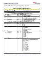
Table 7-41. SRAM-CONFIG Register Field Descriptions
Bit
Field
Type
Reset
Description
15-8
X
X
0h
Don't care
7-0
SRAM-ADDR
R/W
0h
8-bit SRAM address. Writing to this register field configures the
SRAM address to be accessed next. This address automatically
increments after a write to the SRAM.
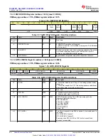
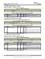
7.6.18 SRAM-DATA Register (address = 2Ch) [reset = 0000h]
PMBus page address = FFh, PMBus register address = F0h
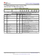
Figure 7-39. SRAM-DATA Register
15
14
13
12
11
10
9
8
7
6
5
4
3
2
1
0
SRAM-DATA
R/W-0h
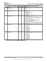
Table 7-42. SRAM-DATA Register Field Descriptions
Bit
Field
Type
Reset
Description
15-0
SRAM-ADDR
R/W
0h
16-bit SRAM data. This data is written to or read from the address
configured in the SRAM-CONFIG register.
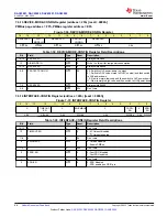
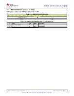
7.6.19 BRDCAST-DATA Register (address = 50h) [reset = 0000h]
PMBus page address = FFh, PMBus register address = F1h
Figure 7-40. BRDCAST-DATA Register
15
14
13
12
11
10
9
8
7
6
5
4
3
2
1
0
DAC6300x: BRDCAST-DATA[11:0]
DAC5300x: BRDCAST-DATA[9:0]
X
R/W-0h
X-0h
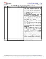
Table 7-43. BRDCAST-DATA Register Field Descriptions
Bit
Field
Type
Reset
Description
15-4
DAC6300x: BRDCAST-DATA[11:0]
DAC5300x: BRDCAST-DATA[9:0]
R/W
000h
Broadcast code for all DAC channels
Data are in straight-binary format. MSB left-aligned. Use the
following bit-alignment:
DAC63001: {DAC-X-MARGIN-HIGH[11:0]}
DAC63002: {DAC-X-MARGIN-HIGH[11:0]}
DAC53001: {DAC-X-MARGIN-HIGH[9:0], X, X}
DAC53002: {DAC-X-MARGIN-HIGH[9:0], X, X}
X = Don't care bits.
The BRD-CONFIG-X bit in the DAC-X-FUNC-CONFIG register
must be enabled for the respective channels.
3-0
X
X
0h
Don't care.
DAC53001, DAC53002, DAC63001, DAC63002
SLASF48 – MAY 2022
Copyright © 2022 Texas Instruments Incorporated
69
Product Folder Links:


