Application Information
(Continued)
Determining Maximum Power Dissipation
Power dissipation within the integrated circuit package is a
very important parameter requiring a thorough understand-
ing if optimum power output is to be obtained. An incorrect
maximum power dissipation (P
D
) calculation may result in
inadequate heat sinking, causing thermal shutdown circuitry
to operate and limit the output power.
The following equations can be used to acccurately calculate
the maximum and average integrated circuit power dissipa-
tion for your amplifier design, given the supply voltage, rated
load, and output power. These equations can be directly
applied to the Power Dissipation vs Output Power curves in
the
Typical Performance Characteristics
section.
Equation (1)
exemplifies the maximum power dissipation of
the IC and
Equations (2), (3)
exemplify the average IC power
dissipation expressed in different forms.
P
DMAX
= V
CC
2/2
π
2
R
L
(1)
where V
CC
is the total supply voltage
P
DAVE
= (V
Opk
/R
L
)[V
CC
/
π
− V
Opk
/2]
(2)
where V
CC
is the total supply voltage and V
Opk
= V
CC
/
π
P
DAVE
= V
CC
V
Opk
/
π
R
L
− V
Opk
2
/2R
L
(3)
where V
CC
is the total supply voltage.
Determining the Correct Heat Sink
Once the maximum IC power dissipation is known for a
given supply voltage, rated load, and the desired rated out-
put power the maximum thermal resistance (in ˚C/W) of a
heat sink can be calculated. This calculation is made using
Equation (4)
and is based on the fact that thermal heat flow
parameters are analogous to electrical current flow proper-
ties.
It is also known that typically the thermal resistance,
θ
JC
(junction to case), of the LM3886 is 1˚C/W and that using
Thermalloy Thermacote thermal compound provides a ther-
mal resistance,
θ
CS
(case to heat sink), of about 0.2˚C/W as
explained in the
Heat Sinking
section.
Referring to the figure below, it is seen that the thermal
resistance from the die (junction) to the outside air (ambient)
is a combination of three thermal resistances, two of which
are known,
θ
JC
and
θ
CS
. Since convection heat flow (power
dissipation) is analogous to current flow, thermal resistance
is analogous to electrical resistance, and temperature drops
are analogous to voltage drops, the power dissipation out of
the LM3886 is equal to the following:
P
DMAX
= (T
Jmax
− T
Amb
)/
θ
JA
where
θ
JA
=
θ
JC
+
θ
CS
+
θ
SA
01183312
But since we know P
DMAX
,
θ
JC
, and
θ
SC
for the application
and we are looking for
θ
SA
, we have the following:
θ
SA
= [(T
Jmax
− T
Amb
) − P
DMAX
(
θ
JC
+
θ
CS
)]/P
DMAX
(4)
Again it must be noted that the value of
θ
SA
is dependent
upon the system designer’s amplifier application and its
corresponding parameters as described previously. If the
ambient temperature that the audio amplifier is to be working
under is higher than the normal 25˚C, then the thermal
resistance for the heat sink, given all other things are equal,
will need to be smaller.
Equations (1), (4)
are the only equations needed in the
determination of the maximum heat sink thermal resistance.
This is of course given that the system designer knows the
required supply voltages to drive his rated load at a particular
power output level and the parameters provided by the
semiconductor manufacturer. These parameters are the
junction to case thermal resistance,
θ
JC
, T
Jmax
= 150˚C, and
the recommended Thermalloy Thermacote thermal com-
pound resistance,
θ
CS
.
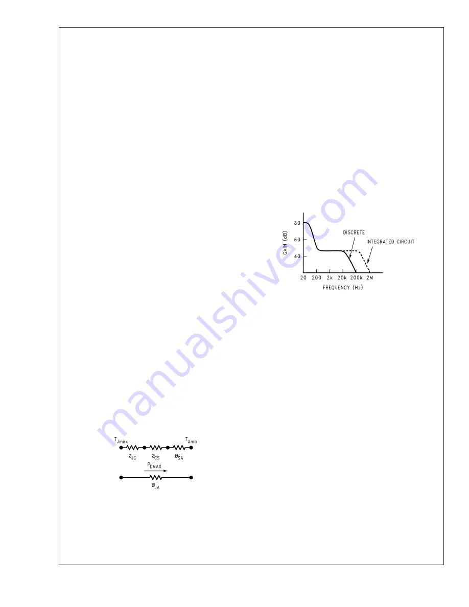
SIGNAL-TO-NOISE RATIO
In the measurement of the signal-to-noise ratio, misinterpre-
tations of the numbers actually measured are common. One
amplifier may sound much quieter than another, but due to
improper testing techniques, they appear equal in measure-
ments. This is often the case when comparing integrated
circuit designs to discrete amplifier designs. Discrete transis-
tor amps often “run out of gain” at high frequencies and
therefore have small bandwidths to noise as indicated below.
01183313
Integrated circuits have additional open loop gain allowing
additional feedback loop gain in order to lower harmonic
distortion and improve frequency response. It is this addi-
tional bandwidth that can lead to erroneous signal-to-noise
measurements if not considered during the measurement
process. In the typical example above, the difference in
bandwidth appears small on a log scale but the factor of 10
in bandwidth, (200 kHz to 2 MHz) can result in a 10 dB
theoretical difference in the signal-to-noise ratio (white noise
is proportional to the square root of the bandwidth in a
system).
In comparing audio amplifiers it is necessary to measure the
magnitude of noise in the audible bandwidth by using a
“weighting” filter (Note 18). A “weighting” filter alters the
frequency response in order to compensate for the average
human ear’s sensitivity to the frequency spectra. The weight-
ing filters at the same time provide the bandwidth limiting as
discussed in the previous paragraph.
Note 18:
CCIR/ARM:
A Practical Noise Measurement Method;
by Ray
Dolby, David Robinson and Kenneth Gundry, AES Preprint No. 1353 (F-3).
In addition to noise filtering, differing meter types give differ-
ent noise readings. Meter responses include:
1.
RMS reading,
2.
average responding,
3.
peak reading, and
4.
quasi peak reading.
Although theoretical noise analysis is derived using true
RMS based calculations, most actual measurements are
taken with ARM (Average Responding Meter) test equip-
ment.
LM3886
www.national.com
18


