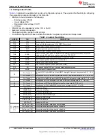
1.2 Configuration Points
indicates the available test points and configuration jumpers. These points offer flexibility in configuring
the evaluation module and include but not limited to:
• BIAS pin to be connected to the following:
– External supply (VAUX)
– Input voltage (VIN)
– Regulated output voltage (VOUT)
– VCC pin
• PGOOD pin to be supplied by either VCC or VAUX
• External clock synchronization
• Shut-down signal by pulling the SD pin high
• Four different operation modes to enable and disable the spread spectrum and hiccup mode
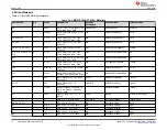
Table 1-2. Jumper Description
JUMPER
PIN
DESCRIPTION
TP1
VIN+
Positive input voltage sense connection
TP2
SW
Probe point for the switch node of the LM5157 boost circuit
TP3
VOUT+
Positive output voltage sense connection
TP4
GND
Negative input voltage sense connection
TP5
GND
Negative output voltage sense connection
TP6
SYNC
Input for external clock signal. To implement the external clock synchronization, remove the
jumper resistor R10 and tie the external signal to the TP6 (SYNC).
TP7
VAUX
Supply the BIAS pin from an external supply (if J9 is connected).
TP8
VOUT+
Loop response positive injection point (bottom side)
TP9
UVLO
Middle point of UVLO resistor divider
TP10
VOUT–
Loop response negative injection point (bottom side)
TP11
SD
High signal pulls the UVLO pin to ground entering shutdown mode
TP12
AGND
Negative input of external signals
J6
Pin 1 to pin 2
Connect VOUT to the BIAS pin of the LM5157 through D2 (only set one jumper to J6, J7, J8, or
J9).
Pin 2 to pin 3
Directly connect VOUT to the BIAS pin of the LM5157 (only set one jumper to J6, J7, J8, or J9).
J7
Pin 1 to pin 2
Connect VIN to the BIAS pin of the LM5157 through D3 (only set one jumper to J6, J7, J8, or J9).
Pin 2 to pin 3
Directly connect VIN to BIAS pin of the LM5157 (only set one jumper to J6, J7, J8, or J9).
J8
Pin 1 to pin 2
Directly connect VCC to the BIAS pin (only set one jumper to J6, J7, J8 or J9).
J9
Pin 1 to pin 2
Directly connect VAUX to the BIAS pin (only set one jumper to J6, J7, J8, or J9).
J10
SS (Pin 1)
Monitor the SS pin.
COMP (Pin 2)
Monitor the COMP pin.
AGND (Pin 3)
Connection to AGND plane
SYNC (Pin 4)
Monitor the EN/UVLO/SYNC pin.
PGOOD (Pin 5)
Monitor the PGOOD pin.
BIAS-IC (Pin 6)
Monitor the BIAS pin.
VCC (Pin 7)
Monitor the VCC pin.
J11 (only use
one jumper on
J11)
Pin 1 to pin 2 (NN)
Hiccup mode disabled, spread spectrum disabled
Pin 3 to pin 4 (HS)
Hiccup mode enabled, spread spectrum enabled
Pin 5 to pin 6 (HN)
Hiccup mode enabled, spread spectrum disabled
Pin 7 to pin 8 (NS)
Hiccup mode disabled, spread spectrum enabled
Features and Electrical Performance
4
LM5157EVM-BST Evaluation Module
SNVU739A – OCTOBER 2020 – REVISED AUGUST 2021
Copyright © 2021 Texas Instruments Incorporated


