background image

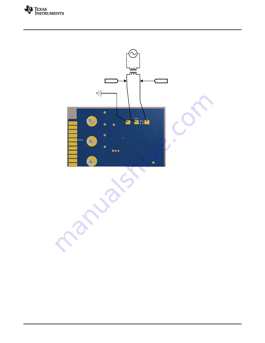
OSC

B

A

Signal 

Injection

³%´ ,QSXW WR

network analyzer

³$´ ,QSXW WR

network analyzer

www.ti.com

Operation

5

SNVU573A – August 2017 – Revised March 2018

Submit Documentation Feedback

Copyright © 2017–2018, Texas Instruments Incorporated

LMR33630 EVM User’s Guide

Figure 4. FRA Set-up

2

Operation

Once the above connections are made and the appropriate jumpers are set, the EVM is ready for use. If
external control of the EN input is desired, remove the EN jumper, and apply the external signal to the EN
test point and GND. The PGOOD output is pulled up to VCC through a 20-k

Ω

resistor. In this way the

PGOOD signal swings from 0 V to about 5 V to indicate when the output voltage is either outside or inside
of the PGOOD window, respectively. If an external pullup and supply is desired for the PGOOD function,
remove the 20-k

Ω

resistor, and pull the PGOOD test point up to the desired voltage through an

appropriate resistance. See the LMR33630 data sheets for more details.

The output voltage of the EVM can be selected, by the VOUT jumper, to either 3.3 V or 5 V. Other values
of output voltage can be programmed by changing the value of R

FBB

on the EVM. In addition the values of

the inductor and the output capacitance may also need to be changed. See the LMR33630 data sheets for
more information.

The EVM has been designed for maximum flexibility regarding component selection. This allows the user
to place prefered components, such as the inductor and/or capacitors, on the board and test the
performance of the regulator. In this way the power supply system can be tested before committing the
design to production.

Summary of Contents for LMR33630ADDAEVM

Page 1: ...et for additional features detailed description and available options The EVM options are found in Table 1 Table 1 Device and Package Configurations EVM DEVICE FREQUENCY Output Current LMR33630ADDAEVM LMR33630ADDA 400 kHz 3A LMR33630CDDAEVM LMR33630CDDA 2100 kHz 3A Contents 1 Setup 2 2 Operation 5 3 Performance Curves 6 4 Schematic 7 5 Board Layout 8 6 Bill of Materials 13 List of Figures 1 EVM Bo...

Page 2: ... the top of the board can be used for connections or the card edge connector can be used Please refer to Figure 1 for the top of board connections and Figure 2 for the card edge connections The following lists the functions of the connections VIN Input supply to EVM Connect to a suitable input supply See LMR33630 data sheets for input supply requirements GND System ground VOUT Output of EVM Connec...

Page 3: ...ser s Guide Figure 2 EVM Card Edge Connections 1 1 Jumpers Please refer to Figure 3 for jumper locations EN This jumper allows the EN input to be connected to either ground OFF or VIN ON Remove this jumper to allow an external logic signal to control the EN function VOUT This jumper is used to select one of the two pre defined output voltages The 3 3V position provides a 3 3 V output while the 5V ...

Page 4: ...tion connect to DMM Also used for frequency response analyzer connection VIS Input voltage sense connection connect to DMM GNDS Ground sense point for analog measurements connect to DMM VCC Test point to measure internal VCC of device approximately 5V On board PGOOD pull up resistor is connected to VCC EN Connection for external EN logic input Remove EN jumper and connect controlling logic to EN t...

Page 5: ...PGOOD window respectively If an external pullup and supply is desired for the PGOOD function remove the 20 kΩ resistor and pull the PGOOD test point up to the desired voltage through an appropriate resistance See the LMR33630 data sheets for more details The output voltage of the EVM can be selected by the VOUT jumper to either 3 3 V or 5 V Other values of output voltage can be programmed by chang...

Page 6: ...1 10 Efficiency Output Current A 5V 3 3V C001 Performance Curves www ti com 6 SNVU573A August 2017 Revised March 2018 Submit Documentation Feedback Copyright 2017 2018 Texas Instruments Incorporated LMR33630 EVM User s Guide 3 Performance Curves Figure 5 Efficiency VIN 12 V ƒSW 2 1 MHz Figure 6 Efficiency VIN 12 V ƒSW 400 kHz ...

Page 7: ...E BOM www ti com Schematic 7 SNVU573A August 2017 Revised March 2018 Submit Documentation Feedback Copyright 2017 2018 Texas Instruments Incorporated LMR33630 EVM User s Guide 4 Schematic Figure 7 LMR33630EVM Schematic ...

Page 8: ... Layout www ti com 8 SNVU573A August 2017 Revised March 2018 Submit Documentation Feedback Copyright 2017 2018 Texas Instruments Incorporated LMR33630 EVM User s Guide 5 Board Layout Figure 8 Top View of EVM ...

Page 9: ...www ti com Board Layout 9 SNVU573A August 2017 Revised March 2018 Submit Documentation Feedback Copyright 2017 2018 Texas Instruments Incorporated LMR33630 EVM User s Guide Figure 9 EVM Top Copper Layer ...

Page 10: ...Board Layout www ti com 10 SNVU573A August 2017 Revised March 2018 Submit Documentation Feedback Copyright 2017 2018 Texas Instruments Incorporated LMR33630 EVM User s Guide Figure 10 EVM Mid Layer One ...

Page 11: ...www ti com Board Layout 11 SNVU573A August 2017 Revised March 2018 Submit Documentation Feedback Copyright 2017 2018 Texas Instruments Incorporated LMR33630 EVM User s Guide Figure 11 EVM Mid Layer Two ...

Page 12: ...rd Layout www ti com 12 SNVU573A August 2017 Revised March 2018 Submit Documentation Feedback Copyright 2017 2018 Texas Instruments Incorporated LMR33630 EVM User s Guide Figure 12 EVM Bottom Copper Layer ...

Page 13: ...R 1210 Samsung CL32A226KAJNNNE 4 J1 J2 J3 Standard Banana Jack Uninsulated 8 9mm Keystone 575 8 3 J4 J5 Header 100mil 3x1 Gold TH Samtec HTSW 103 07 G S 2 L1 Inductor Shielded Drum Core Ferrite 8 2 µH 8 A 0 0132 ohm SMD Wurth Elektronik 7443330820 1 Rinj RES 10 0 1 0 1 W 0603 Vishay Dale CRCW060310R0FKEA 1 RFBT2 RES 34 0 k 1 0 1 W 0603 Yageo America RC0603FR 0734KL 1 RFBT1 RES 46 4 k 1 0 1 W 0603 ...

Page 14: ...sung CL32A226KAJNNNE 4 J1 J2 J3 Standard Banana Jack Uninsulated 8 9mm Keystone 575 8 3 J4 J5 Header 100mil 3x1 Gold TH Samtec HTSW 103 07 G S 2 L1 Inductor Shielded Drum Core Ferrite 1 5 µH 18 A 0 0025 ohm SMD Wurth Elektronik 7443330150 1 Rinj RES 10 0 1 0 1 W 0603 Vishay Dale CRCW060310R0FKEA 1 RFBT2 RES 34 0 k 1 0 1 W 0603 Yageo America RC0603FR 0734KL 1 RFBT1 RES 46 4 k 1 0 1 W 0603 Yageo Ame...

Page 15: ...mit Documentation Feedback Copyright 2017 2018 Texas Instruments Incorporated Revision History Revision History NOTE Page numbers for previous revisions may differ from page numbers in the current version Changes from Original August 2017 to A Revision Page Added Section 3 5 ...

Page 16: ...y set forth above or credit User s account for such EVM TI s liability under this warranty shall be limited to EVMs that are returned during the warranty period to the address designated by TI and that are determined by TI not to conform to such warranty If TI elects to repair or replace such EVM TI shall have a reasonable time to repair such EVM or provide replacements Repaired EVMs shall be warr...

Page 17: ...the user guide with the maximum permissible gain and required antenna impedance for each antenna type indicated Antenna types not included in this list having a gain greater than the maximum gain indicated for that type are strictly prohibited for use with this device Concernant les EVMs avec antennes détachables Conformément à la réglementation d Industrie Canada le présent émetteur radio peut fo...

Page 18: ...ed loads Any loads applied outside of the specified output range may also result in unintended and or inaccurate operation and or possible permanent damage to the EVM and or interface electronics Please consult the EVM user guide prior to connecting any load to the EVM output If there is uncertainty as to the load specification please contact a TI field representative During normal operation even ...

Page 19: ...COST OF REMOVAL OR REINSTALLATION ANCILLARY COSTS TO THE PROCUREMENT OF SUBSTITUTE GOODS OR SERVICES RETESTING OUTSIDE COMPUTER TIME LABOR COSTS LOSS OF GOODWILL LOSS OF PROFITS LOSS OF SAVINGS LOSS OF USE LOSS OF DATA OR BUSINESS INTERRUPTION NO CLAIM SUIT OR ACTION SHALL BE BROUGHT AGAINST TI MORE THAN TWELVE 12 MONTHS AFTER THE EVENT THAT GAVE RISE TO THE CAUSE OF ACTION HAS OCCURRED 8 2 Specif...

Page 20: ... TI Resource NO OTHER LICENSE EXPRESS OR IMPLIED BY ESTOPPEL OR OTHERWISE TO ANY OTHER TI INTELLECTUAL PROPERTY RIGHT AND NO LICENSE TO ANY TECHNOLOGY OR INTELLECTUAL PROPERTY RIGHT OF TI OR ANY THIRD PARTY IS GRANTED HEREIN including but not limited to any patent right copyright mask work right or other intellectual property right relating to any combination machine or process in which TI product...

Reviews: