background image

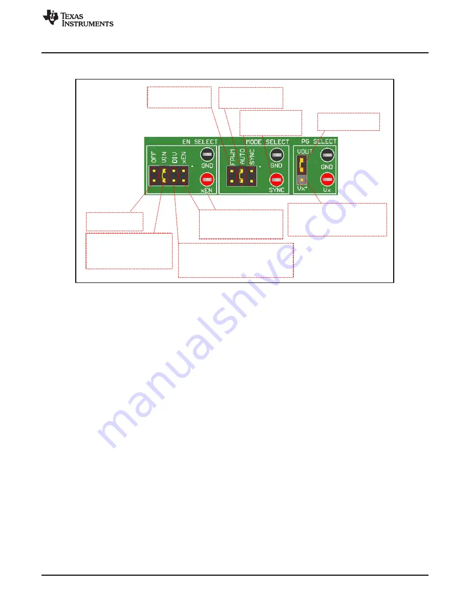
EN connected to GND 

The converter is OFF

EN connected to VIN


The converter is ON when the VIN 

voltage is above the VIN UVLO 

rising threshold

EN connected to VIN through a resistor divider

The converter is ON when the divider voltage is 

above the EN rising threshold and the VIN 

voltage is above the VIN UVLO 

EN connected to the xEN terminal

 Provide enable signal at the xEN 

to turn the device ON

MODE connected to VIN


FPWM is enabled

MODE connected to GND


Auto PFM is enabled

Provide external clock at 

SYNC to synchronize the 

switching frequency

PGOOD pullup voltage 

connected to VOUT

PGOOD pullup voltage connected to Vx

Provide external voltage at Vx for the 

PGOOD flag logic HIGH level

www.ti.com

Getting Started

5

SNVU578A – October 2017 – Revised March 2018

Submit Documentation Feedback

Copyright © 2017–2018, Texas Instruments Incorporated

User's Guide for the LMZM23601 and LMZM23600 Evaluation Boards

Figure 3. Jumper Configuration Details for Each Board

Before applying power to the EVM, ensure that all of the jumpers are in place and are properly positioned
for the intended feature setting and output voltage operation. Always shut down the input power supply
before changing any of the jumper settings.

Figure 1

and

Figure 3

above provide an overview of the board

connection terminals, jumper setting options, and test points.

Use the "VIN POWER TERMINAL" and "GND TERMINAL" turrets to connect the board to the input
supply. Connect the load between the "VOUT TERMINAL" and "GND TERMINAL".

For the adjustable output version of the board, the output voltage setting jumper configures the feedback
resistor divider pair for various popular output voltages: 2.5 V, 3.3 V, 5 V, 12 V, or 15 V. Voltage sense
points are provided to help read the input voltage and output voltage directly at the regulator. The sense
lines should not be used for power connections. There are several test points provided on the left hand
side of the board. They can be used to monitor the voltage signals at the MODE, EN, and PG pins of the
device.

The EN selection jumper allows the user to select the desired enabling scheme for the end application.
The LMZM23600 and LMZM23601 feature a precision enable input which can be used to set the input
UVLO point with a voltage divider from the input voltage. Alternatively, the enable input can be driven by a
logic signal or it could be tied directly to VIN for an always-on operation.

The MODE selection jumper sets the DC/DC converter mode of operation at light load. When Auto PFM
mode is selected, the converter will enter PFM mode at light load and reduce the switching frequency in
order to maintain high conversion efficiency. Some applications may require that the regulator maintains
constant switching frequency across the entire load range. In such cases the mode pin can be used to set
forced PWM operation at light load. The mode terminal can also be used to synchronize the converter
switching frequency to an external clock. If frequency synchronization is used, the converter will operate in
forced PWM mode at light load.

The PGOOD flag jumper allows the user to either connect the PGOOD pullup resistor to VOUT or provide
an external voltage rail for the logic HIGH voltage level.

Summary of Contents for LMZM23600

Page 1: ... VOUT 12 V 11 5 3 VOUT 5 V 12 5 4 VOUT 3 3 V 13 5 5 VOUT 2 5 V 14 6 PCB Layout 15 6 1 Adjustable Output Voltage Versions 15 6 2 Fixed Output Voltage Versions 19 List of Figures 1 EVM User Interface for the Adjustable Output Voltage Options 4 2 EVM User Interface for the Fixed 5 V and 3 3 V Output Voltage Options 4 3 Jumper Configuration Details for Each Board 5 4 Schematic for the Adjustable Outpu...

Page 2: ...able Output Board Layout Top Overlay 15 29 Adjustable Output Board Layout Top Soldermask 15 30 Adjustable Output Board Layout Top Layer Copper 16 31 Adjustable Output Board Layout Mid Layer 1 under top layer Copper 16 32 Adjustable Output Board Layout Mid Layer 2 above bottom layer Copper 17 33 Adjustable Output Board Layout Bottom Layer Copper 17 34 Adjustable Output Board Layout Bottom Soldermas...

Page 3: ...ils about the operating range features and specifications of the LMZM23601 and LMZM23600 can be found in the device data sheet The output voltage for the adjustable ADJ version can be configured between 2 5 V and 15 V There are also fixed output options of the devices for 5 V and 3 3 V outputs and each voltage option comes in two output current choices 0 5 A and 1 A There are two main evaluation b...

Page 4: ...TS ENABLE CONNECTION JUMPER MODE SELECTION JUMPER PGOOD FLAG PULLUP VOLTAGE JUMPER OUTPUT VOLTAGE SETTING JUMPER Getting Started www ti com 4 SNVU578A October 2017 Revised March 2018 Submit Documentation Feedback Copyright 2017 2018 Texas Instruments Incorporated User s Guide for the LMZM23601 and LMZM23600 Evaluation Boards 2 Getting Started Figure 1 EVM User Interface for the Adjustable Output V...

Page 5: ...stable output version of the board the output voltage setting jumper configures the feedback resistor divider pair for various popular output voltages 2 5 V 3 3 V 5 V 12 V or 15 V Voltage sense points are provided to help read the input voltage and output voltage directly at the regulator The sense lines should not be used for power connections There are several test points provided on the left ha...

Page 6: ... March 2018 Submit Documentation Feedback Copyright 2017 2018 Texas Instruments Incorporated User s Guide for the LMZM23601 and LMZM23600 Evaluation Boards 3 Schematic 3 1 Adjustable Output Voltage Versions Figure 4 Schematic for the Adjustable Output Voltage Versions of the Module ...

Page 7: ...SNVU578A October 2017 Revised March 2018 Submit Documentation Feedback Copyright 2017 2018 Texas Instruments Incorporated User s Guide for the LMZM23601 and LMZM23600 Evaluation Boards 3 2 Fixed Output Voltage Versions Figure 5 Schematic for the Fixed Output Voltage Versions of the Module ...

Page 8: ...CRCW0402178KFKED Vishay Dale R6 1 76 8k Resistor 76 8 k 1 0 063 W 0402 CRCW040276K8FKED Vishay Dale R7 1 887k Resistor 887 k 1 0 1 W 0603 CRCW0603887KFKEA Vishay Dale R8 R9 2 100k Resistor 100 k 1 0 1 W 0603 CRCW0603100KFKEA Vishay Dale SH J1 SH J2 SH J3 SH J4 4 1x2 Shunt 100mil Gold plated Black SNT 100 BK G Samtec TP1 TP2 TP3 3 Terminal Turret TH Triple 1598 2 Keystone TP4 TP6 TP9 TP10 TP12 TP13...

Page 9: ...rch 2018 Submit Documentation Feedback Copyright 2017 2018 Texas Instruments Incorporated User s Guide for the LMZM23601 and LMZM23600 Evaluation Boards 4 2 Fixed Output Voltage Versions Figure 7 Bill Of Materials for the Fixed Output Voltage Versions of the Module ...

Page 10: ...com 10 SNVU578A October 2017 Revised March 2018 Submit Documentation Feedback Copyright 2017 2018 Texas Instruments Incorporated User s Guide for the LMZM23601 and LMZM23600 Evaluation Boards 5 Performance Data The following section demonstrates the LMZM23601 evaluation board performance using the adjustable output voltage option of the device 5 1 VOUT 15 V Figure 8 Efficiency for VOUT 15 V Figure...

Page 11: ...N 24 V PFM VIN 24 V FPWM VIN 36 V PFM VIN 36 V FPWM www ti com Performance Data 11 SNVU578A October 2017 Revised March 2018 Submit Documentation Feedback Copyright 2017 2018 Texas Instruments Incorporated User s Guide for the LMZM23601 and LMZM23600 Evaluation Boards 5 2 VOUT 12 V Figure 12 Efficiency for VOUT 12 V Figure 13 Load Transient Response for VOUT 12 V 10 to 100 Load Step FPWM Figure 14 ...

Page 12: ... VIN 24 V PFM VIN 24 V FPWM VIN 36 V PFM VIN 36 V FPWM Performance Data www ti com 12 SNVU578A October 2017 Revised March 2018 Submit Documentation Feedback Copyright 2017 2018 Texas Instruments Incorporated User s Guide for the LMZM23601 and LMZM23600 Evaluation Boards 5 3 VOUT 5 V Figure 16 Efficiency for VOUT 5 V Figure 17 Load Transient Response for VOUT 5 V 10 to 100 Load Step FPWM Figure 18 ...

Page 13: ...4 V PFM VIN 24 V FPWM VIN 36 V PFM VIN 36 V FPWM www ti com Performance Data 13 SNVU578A October 2017 Revised March 2018 Submit Documentation Feedback Copyright 2017 2018 Texas Instruments Incorporated User s Guide for the LMZM23601 and LMZM23600 Evaluation Boards 5 4 VOUT 3 3 V Figure 20 Efficiency for VOUT 3 3 V Figure 21 Load Transient Response for VOUT 3 3 V 10 to 100 Load Step FPWM Figure 22 ...

Page 14: ...4 V PFM VIN 24 V FPWM VIN 36 V PFM VIN 36 V FPWM Performance Data www ti com 14 SNVU578A October 2017 Revised March 2018 Submit Documentation Feedback Copyright 2017 2018 Texas Instruments Incorporated User s Guide for the LMZM23601 and LMZM23600 Evaluation Boards 5 5 VOUT 2 5 V Figure 24 Efficiency for VOUT 2 5 V Figure 25 Load Transient Response for VOUT 2 5 V 10 to 100 Load Step FPWM Figure 26 ...

Page 15: ...ation Boards 6 PCB Layout This section of the user s guide describes the PCB layout of the LMZM23601 boards The layout is the same for the LMZM23600 versions The boards have 4 copper layers The boards dimensions are 58 mm 2 3 inches 70 mm 2 75 inches 6 1 Adjustable Output Voltage Versions Figure 28 Adjustable Output Board Layout Top Overlay Figure 29 Adjustable Output Board Layout Top Soldermask ...

Page 16: ...t Documentation Feedback Copyright 2017 2018 Texas Instruments Incorporated User s Guide for the LMZM23601 and LMZM23600 Evaluation Boards Figure 30 Adjustable Output Board Layout Top Layer Copper Figure 31 Adjustable Output Board Layout Mid Layer 1 under top layer Copper ...

Page 17: ...ocumentation Feedback Copyright 2017 2018 Texas Instruments Incorporated User s Guide for the LMZM23601 and LMZM23600 Evaluation Boards Figure 32 Adjustable Output Board Layout Mid Layer 2 above bottom layer Copper Figure 33 Adjustable Output Board Layout Bottom Layer Copper ...

Page 18: ...2018 Submit Documentation Feedback Copyright 2017 2018 Texas Instruments Incorporated User s Guide for the LMZM23601 and LMZM23600 Evaluation Boards Figure 34 Adjustable Output Board Layout Bottom Soldermask Figure 35 Adjustable Output Board Layout Bottom Overlay ...

Page 19: ...it Documentation Feedback Copyright 2017 2018 Texas Instruments Incorporated User s Guide for the LMZM23601 and LMZM23600 Evaluation Boards 6 2 Fixed Output Voltage Versions Figure 36 Fixed Output Board Layout Top Overlay Figure 37 Fixed Output Board Layout Top Soldermask ...

Page 20: ...Submit Documentation Feedback Copyright 2017 2018 Texas Instruments Incorporated User s Guide for the LMZM23601 and LMZM23600 Evaluation Boards Figure 38 Fixed Output Board Layout Top Layer Copper Figure 39 Fixed Output Board Layout Mid Layer 1 under top layer Copper ...

Page 21: ...mit Documentation Feedback Copyright 2017 2018 Texas Instruments Incorporated User s Guide for the LMZM23601 and LMZM23600 Evaluation Boards Figure 40 Fixed Output Board Layout Mid Layer 2 above bottom layer Copper Figure 41 Fixed Output Board Layout Bottom Layer Copper ...

Page 22: ...arch 2018 Submit Documentation Feedback Copyright 2017 2018 Texas Instruments Incorporated User s Guide for the LMZM23601 and LMZM23600 Evaluation Boards Figure 42 Fixed Output Board Layout Bottom Soldermask Figure 43 Fixed Output Board Layout Bottom Overlay ...

Page 23: ...17 2018 Texas Instruments Incorporated Revision History Revision History NOTE Page numbers for previous revisions may differ from page numbers in the current version Changes from Original October 2017 to A Revision Page Changed title made updates throughout document to include all board options for module family 1 ...

Page 24: ...y set forth above or credit User s account for such EVM TI s liability under this warranty shall be limited to EVMs that are returned during the warranty period to the address designated by TI and that are determined by TI not to conform to such warranty If TI elects to repair or replace such EVM TI shall have a reasonable time to repair such EVM or provide replacements Repaired EVMs shall be warr...

Page 25: ...the user guide with the maximum permissible gain and required antenna impedance for each antenna type indicated Antenna types not included in this list having a gain greater than the maximum gain indicated for that type are strictly prohibited for use with this device Concernant les EVMs avec antennes détachables Conformément à la réglementation d Industrie Canada le présent émetteur radio peut fo...

Page 26: ...ed loads Any loads applied outside of the specified output range may also result in unintended and or inaccurate operation and or possible permanent damage to the EVM and or interface electronics Please consult the EVM user guide prior to connecting any load to the EVM output If there is uncertainty as to the load specification please contact a TI field representative During normal operation even ...

Page 27: ...COST OF REMOVAL OR REINSTALLATION ANCILLARY COSTS TO THE PROCUREMENT OF SUBSTITUTE GOODS OR SERVICES RETESTING OUTSIDE COMPUTER TIME LABOR COSTS LOSS OF GOODWILL LOSS OF PROFITS LOSS OF SAVINGS LOSS OF USE LOSS OF DATA OR BUSINESS INTERRUPTION NO CLAIM SUIT OR ACTION SHALL BE BROUGHT AGAINST TI MORE THAN TWELVE 12 MONTHS AFTER THE EVENT THAT GAVE RISE TO THE CAUSE OF ACTION HAS OCCURRED 8 2 Specif...

Page 28: ... TI Resource NO OTHER LICENSE EXPRESS OR IMPLIED BY ESTOPPEL OR OTHERWISE TO ANY OTHER TI INTELLECTUAL PROPERTY RIGHT AND NO LICENSE TO ANY TECHNOLOGY OR INTELLECTUAL PROPERTY RIGHT OF TI OR ANY THIRD PARTY IS GRANTED HEREIN including but not limited to any patent right copyright mask work right or other intellectual property right relating to any combination machine or process in which TI product...

Reviews: