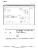
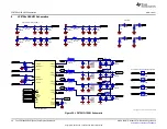
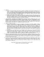
background image

www.ti.com

Board Layout

29

SNVU472B – October 2016 – Revised August 2018

Submit Documentation Feedback

Copyright © 2016–2018, Texas Instruments Incorporated

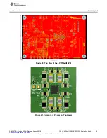
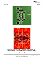
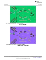
The LP8756xQ1EVM (SV601325) Evaluation Module

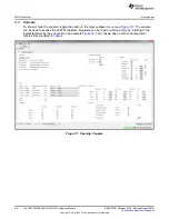
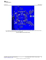
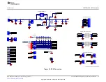
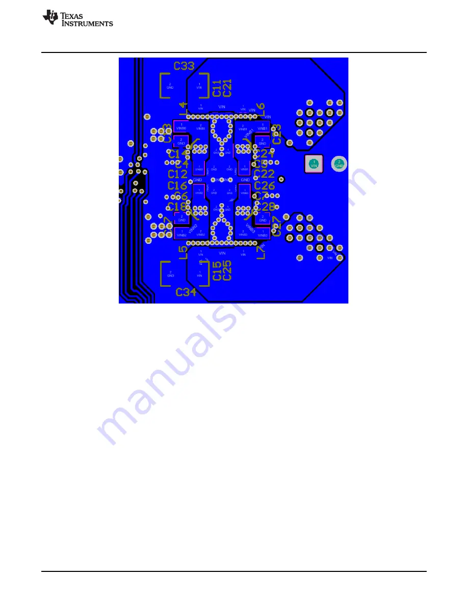
Input capacitors and filters are placed under the LP8756xQ1 into bottom layer. This allows closer placement of the inductors and input
components reducing SW and VIN net areas and improving EMI.

Figure 28. Bottom Layer (note mirror view)

Summary of Contents for LP8756 Q1EVM Series

Page 1: ...r s guide also provides design information including the schematic and bill of materials BOM Contents 1 Overview 3 2 Quick Setup Guide 3 2 1 Installing Opening the Software 4 2 2 Power Supply Setup 8 2 3 Notes on Efficiency Measurement Procedure 12 3 GUI Overview 12 3 1 Main Tab 12 3 2 Other Tabs and Menus 13 3 3 Console 20 4 Bill of Materials 22 5 Board Layout 24 6 LP8756xQ1EVM Schematics 30 List...

Page 2: ...t Bottom Layer 26 23 Top Layer 26 24 Mid Layer1 26 25 Mid Layer2 27 26 Mid Layer3 27 27 Mid Layer4 GND Plane 28 28 Bottom Layer note mirror view 28 29 LP87561Q1EVM Schematic 30 30 LP87562Q1EVM Schematic 31 31 LP87563Q1EVM 32 32 LP87564Q1EVM Schematic 33 33 LP87565Q1EVM Schematic 34 34 EVM Connectors 35 35 EVM I2 C Interface 36 List of Tables 1 LP8756xQ1 Configurations 3 2 Mode Information 13 3 I2 ...

Page 3: ...se buck converter and four single phase buck converters This document covers user software provided with the EVM and design documentation that includes schematics and parts list Table 1 LP8756xQ1 Configurations PART NUMBER OUTPUT CONFIGURATION NUMBER OF OUTPUTS EVM NUMBER LP87561Q1 4 phase 1 LP87561Q1EVM LP87562Q1 3 phase 1 phase 2 LP87562Q1EVM LP87563Q1 2 phase 1 phase 1 phase 3 LP87563Q1EVM LP87...

Page 4: ...t Windows XP or newer operating system Available USB port Mouse Software installation 1 Open the LP8756_installer exe 2 Installer prompts to accept the license agreement see Figure 2 3 Installer prompts to choose which features of LP8756x Installer you want to install see Figure 3 4 Installer prompts to select Destination Folder see Figure 4 5 Press Install and the installation starts 6 Installer ...

Page 5: ...72B October 2016 Revised August 2018 Submit Documentation Feedback Copyright 2016 2018 Texas Instruments Incorporated The LP8756xQ1EVM SV601325 Evaluation Module Figure 3 Features of LP8756 Installation Figure 4 LP8756 Destination Folder ...

Page 6: ... www ti com 6 SNVU472B October 2016 Revised August 2018 Submit Documentation Feedback Copyright 2016 2018 Texas Instruments Incorporated The LP8756xQ1EVM SV601325 Evaluation Module Figure 5 LP8756 Installation Complete ...

Page 7: ...2B October 2016 Revised August 2018 Submit Documentation Feedback Copyright 2016 2018 Texas Instruments Incorporated The LP8756xQ1EVM SV601325 Evaluation Module Figure 6 Evaluation Software Graphical User Interface GUI When Board Connected ...

Page 8: ...minal block Check that jumpers on the boards are set as shown in Figure 1 factory default jumper configuration Set power supply output ON and then continue with the following steps Note that following steps are only an example Register values enable control mode and multiphase status may differ depending on the LP8756xQ1EVM configuration 1 On Evaluation software GUI click on Assert NRST see Figure...

Page 9: ...ck Setup Guide 9 SNVU472B October 2016 Revised August 2018 Submit Documentation Feedback Copyright 2016 2018 Texas Instruments Incorporated The LP8756xQ1EVM SV601325 Evaluation Module Figure 8 Read Registers Buttons ...

Page 10: ...p Guide www ti com 10 SNVU472B October 2016 Revised August 2018 Submit Documentation Feedback Copyright 2016 2018 Texas Instruments Incorporated The LP8756xQ1EVM SV601325 Evaluation Module Figure 9 BUCK0 Enabled ...

Page 11: ...m Quick Setup Guide 11 SNVU472B October 2016 Revised August 2018 Submit Documentation Feedback Copyright 2016 2018 Texas Instruments Incorporated The LP8756xQ1EVM SV601325 Evaluation Module Figure 10 Assert EN1 ...

Page 12: ...n Config and Advanced The three tabs together provide the user access to the whole register map of the LP8756x Additional register control can be obtained from Tools Direct Register Access 3 1 Main Tab The Main tab see for example Figure 10 has the elemental controls for the EVM and provides a view to the chip status Starting from top the main controls are I2C mode or 4 Enable mode If this states ...

Page 13: ...ar button At the bottom of the GUI window is the Auto Write checkbox If Auto Write is checked default any checking un checking or pulldown menu selections will immediately launch I2 C writes to the chip register s If not checked the user can update the chip registers to correspond the configuration selected on the GUI by clicking Write Registers If Poll Status is selected the software sends a quer...

Page 14: ...ti com 14 SNVU472B October 2016 Revised August 2018 Submit Documentation Feedback Copyright 2016 2018 Texas Instruments Incorporated The LP8756xQ1EVM SV601325 Evaluation Module Figure 11 Accessing Direct Register Write ...

Page 15: ...Overview 15 SNVU472B October 2016 Revised August 2018 Submit Documentation Feedback Copyright 2016 2018 Texas Instruments Incorporated The LP8756xQ1EVM SV601325 Evaluation Module Figure 12 Direct Register Access View ...

Page 16: ...ww ti com 16 SNVU472B October 2016 Revised August 2018 Submit Documentation Feedback Copyright 2016 2018 Texas Instruments Incorporated The LP8756xQ1EVM SV601325 Evaluation Module Figure 13 Selecting Register Values ...

Page 17: ...odule Figure 14 Register Update Mode The Config and Advanced tabs provide the user with pulldown menus and check boxes for the part of the register space that is not covered by the Main tab such as output voltage control These controls are self explanatory Refer to the LP8756xQ1 data sheet for explanation of the functions See following images for reference of the Config and Advanced tabs ...

Page 18: ...w ti com 18 SNVU472B October 2016 Revised August 2018 Submit Documentation Feedback Copyright 2016 2018 Texas Instruments Incorporated The LP8756xQ1EVM SV601325 Evaluation Module Figure 15 Config Tab of the LP8756 GUI ...

Page 19: ... Overview 19 SNVU472B October 2016 Revised August 2018 Submit Documentation Feedback Copyright 2016 2018 Texas Instruments Incorporated The LP8756xQ1EVM SV601325 Evaluation Module Figure 16 Advanced Tab of LP8756 GUI ...

Page 20: ...uation Module 3 3 Console To show or hide the console toggle the option in the View pulldown menu see Figure 17 The console can be used to access the LP8756 registers Registers can be read or written simply by referring to the logical registers by their name See an example Figure 18 The console has a number of integrated macros that are listed in Table 4 Figure 17 Opening Console ...

Page 21: ...register value The logical register names are the same as given in the data sheet and must be in uppercase Example BUCK0_VSET 40 wait time Wait for time given in ms Useful in loops iout buck number Returns the measured load current of the chosen buck core 0x address data or address bits data I2 C read or write command addr value examples 0x12 0xaa 0x12 7 1 0x12 3 0 15 The console supports use of s...

Page 22: ... 10 X7R 0603 MuRata GRM188R71C104KA01D 5 C0_3 C1_3 C2_3 C3_3 CAP CERM 3300 pF 50 V 10 X7R 0402 MuRata GRM155R71H332KA01D 4 C4 C5 C6 C7 CAP CERM 10 µF 10 V 10 X7R 0805_140 MuRata GCM21BR71A106KE22L 4 C8 C14 C18 C24 C28 CAP CERM 0 1 µF 16 V 5 X7R 0402 MuRata GRM155R71C104JA88D 5 C9 C10 C19 C20 CAP CERM 390 pF 50 V 10 X7R 0402 MuRata GRM155R71H391KA01D 4 C11 C15 C21 C25 CAP CERM 6800 pF 50 V 10 X7R 0...

Page 23: ...3FR 076K8L 1 R25 R26 RES 39 0 1 0 1 W 0603 Yageo America RC0603FR 0739RL 2 R27 RES 68 0 k 1 0 1 W 0603 Yageo America RC0603FR 0768KL 1 R28 RES 33 0 k 1 0 1 W 0603 Yageo America RC0603FR 0733KL 1 R29 RES 1 00 1 0 1 W 0603 Yageo America RC0603FR 071RL 1 R30 RES 470 k 5 0 1 W 0603 Vishay Dale CRCW0603470KJNEA 1 R31 R32 RES 1 00 k 1 0 1 W 0603 Vishay Dale CRCW06031K00FKEA 2 SH J1 SH J2 SH J3 SH J4 Shu...

Page 24: ...The board is constructed on a 6 layer PCB using 60 µm copper on top and bottom layers to reduce resistance and improve heat transfer Similar layout can be done as a 4 layer board but 6 layers were chosen to improve grounding and reduce DC resistance Board stack up is shown in Figure 19 Figure 20 shows the top view of the entire board and Figure 21 through Figure 28 show the component placement lay...

Page 25: ... October 2016 Revised August 2018 Submit Documentation Feedback Copyright 2016 2018 Texas Instruments Incorporated The LP8756xQ1EVM SV601325 Evaluation Module Figure 20 Top View of the LP8756xQ1EVM Figure 21 Component Placement Top Layer ...

Page 26: ...6xQ1EVM SV601325 Evaluation Module Figure 22 Component Placement Bottom Layer VIN nets are connected to bottom layer with multiple vias This allows closer placement of the inductors thus reducing SW node size and EMI Also snubber circuits are placed next to SW nets for EMI reduction Multiple GND vias are used to provide solid ground around the LP8756xQ1 device Figure 23 Top Layer ...

Page 27: ...yer 0 063 mm helps to reduce parasitic inductance Holes in the plane are under inductor footprint SW node to reduce parasitic capacitance of the SW node thus reducing noise coupling and improving efficiency Figure 24 Mid Layer1 VIN supply is routed in this layer between the ground planes to reduce radiated emissions VIN and GND vias are placed in hatched pattern to avoid large gaps in these planes...

Page 28: ...edback Copyright 2016 2018 Texas Instruments Incorporated The LP8756xQ1EVM SV601325 Evaluation Module This layer is similar to mid layer2 to reduce resistance of the VIN net Figure 26 Mid Layer3 Placed close to bottom layer 0 063 mm to reduce parasitic inductance Figure 27 Mid Layer4 GND Plane ...

Page 29: ...6 2018 Texas Instruments Incorporated The LP8756xQ1EVM SV601325 Evaluation Module Input capacitors and filters are placed under the LP8756xQ1 into bottom layer This allows closer placement of the inductors and input components reducing SW and VIN net areas and improving EMI Figure 28 Bottom Layer note mirror view ...

Page 30: ...20 3300pF C0_3 3300pF C1_3 3300pF C2_3 3300pF C3_3 Input filters for reducing EMI Snubbers VDDA 30 ohm L4 BLM21PG300SH1D 30 ohm L6 BLM21PG300SH1D 30 ohm L5 BLM21PG300SH1D 30 ohm L7 BLM21PG300SH1D 470nH L0 470nH L1 470nH L2 470nH L3 J01 S1911 46R J021 S1911 46R J23 S1911 46R VOUT0 VOUT2 VOUT2 VOUT1 VOUT3 VOUT0 J022 S1911 46R VOUT2 VOUT0 Shunts for Connecting Phases Together 0 1µF C8 0 1µF C14 0 1µF...

Page 31: ... R4 390pF C20 3300pF C0_3 3300pF C1_3 3300pF C2_3 3300pF C3_3 Input filters for reducing EMI Snubbers VDDA 30 ohm L4 BLM21PG300SH1D 30 ohm L6 BLM21PG300SH1D 30 ohm L5 BLM21PG300SH1D 30 ohm L7 BLM21PG300SH1D 470nH L0 470nH L1 470nH L2 470nH L3 J01 S1911 46R J021 S1911 46R J23 S1911 46R DNP VOUT0 VOUT2 VOUT2 VOUT1 VOUT3 VOUT0 J022 S1911 46R VOUT2 VOUT0 Shunts for Connecting Phases Together 0 1µF C8 ...

Page 32: ...9 R4 390pF C20 3300pF C0_3 3300pF C1_3 3300pF C2_3 3300pF C3_3 Input filters for reducing EMI Snubbers VDDA 30 ohm L4 BLM21PG300SH1D 30 ohm L6 BLM21PG300SH1D 30 ohm L5 BLM21PG300SH1D 30 ohm L7 BLM21PG300SH1D 470nH L0 470nH L1 470nH L2 470nH L3 J01 S1911 46R J021 S1911 46R DNP J23 S1911 46R DNP VOUT0 VOUT2 VOUT2 VOUT1 VOUT3 VOUT0 J022 S1911 46R DNP VOUT2 VOUT0 Shunts for Connecting Phases Together ...

Page 33: ...0pF C20 3300pF C0_3 3300pF C1_3 3300pF C2_3 3300pF C3_3 Input filters for reducing EMI Snubbers VDDA 30 ohm L4 BLM21PG300SH1D 30 ohm L6 BLM21PG300SH1D 30 ohm L5 BLM21PG300SH1D 30 ohm L7 BLM21PG300SH1D 470nH L0 470nH L1 470nH L2 470nH L3 J01 S1911 46R DNP J021 S1911 46R DNP J23 S1911 46R DNP VOUT0 VOUT2 VOUT2 VOUT1 VOUT3 VOUT0 J022 S1911 46R DNP VOUT2 VOUT0 Shunts for Connecting Phases Together 0 1...

Page 34: ...4 390pF C20 3300pF C0_3 3300pF C1_3 3300pF C2_3 3300pF C3_3 Input filters for reducing EMI Snubbers VDDA 30 ohm L4 BLM21PG300SH1D 30 ohm L6 BLM21PG300SH1D 30 ohm L5 BLM21PG300SH1D 30 ohm L7 BLM21PG300SH1D 470nH L0 470nH L1 470nH L2 470nH L3 J01 S1911 46R J021 S1911 46R DNP J23 S1911 46R VOUT0 VOUT2 VOUT2 VOUT1 VOUT3 VOUT0 J022 S1911 46R DNP VOUT2 VOUT0 Shunts for Connecting Phases Together 0 1µF C...

Page 35: ...651712 1 DNP 1 2 3 4 5 6 X6 6651712 1 DNP VOUT0 VOUT1 VOUT3 VOUT2 GND GND Feedback Connector 5 4 1 2 3 6 7 8 X2 GND FB0 FB1 FB2 FB3 1 8k R7 DNP 1 8k R8 DNP 1 8k R9 DNP 0 R14 0 R15 0 R16 0 R17 0 R18 0 R19 DNP SDA SCL HSI2C_SYS 0 R6 DNP 0 R21 0 R22 0 R20 1 8k R10 DNP 1 2 J7 1 2 J8 50 R23 DNP VCC1V8 INTB2B NRSTB2B EN1B2B EN2B2B EN3B2B PGOODB2B CLKINB2B SDASYS SCLSYS INT NRST PGOOD CLKIN EN1 EN2 EN3 E...

Page 36: ...GMD1 38 PB0 90 PB1 91 PB10 70 PB11 93 PB12 94 PB13 95 PB14 69 PB15 16 PB16 15 PB17 68 PB18 67 PB19 66 PB2 92 PB20 65 PB21 64 PB22 63 PB23 62 PB24 58 PB3 7 PB4 8 PB5 97 PB6 98 PB7 99 PB8 100 PB9 71 U2A ATSAM3U2CA AU DHSDP 76 DHSDM 77 FWUP 42 NRST 57 XOUT32 49 TST 44 ERASE 43 NRSTB 47 XIN32 50 XOUT 74 XIN 75 VBG 78 DFSDM 80 DFSDP 81 VDDUTMI 79 GNDUTMI 82 U2B ATSAM3U2CA AU LDO1 1 8 V 150 mA VDDIO for...

Page 37: ... differ from page numbers in the current version Changes from Original October 2016 to A Revision Page Added caution graphic 1 Changed Changed number of outputs for LP87525Q1 from 5 to 2 3 Revision History Changes from A Revision February 2017 to B Revision Page Added SV601325 to the title to indicate which EVM version it applies to 1 Added link to the newer BMC031 version of this document 1 Added...

Page 38: ...y set forth above or credit User s account for such EVM TI s liability under this warranty shall be limited to EVMs that are returned during the warranty period to the address designated by TI and that are determined by TI not to conform to such warranty If TI elects to repair or replace such EVM TI shall have a reasonable time to repair such EVM or provide replacements Repaired EVMs shall be warr...

Page 39: ...the user guide with the maximum permissible gain and required antenna impedance for each antenna type indicated Antenna types not included in this list having a gain greater than the maximum gain indicated for that type are strictly prohibited for use with this device Concernant les EVMs avec antennes détachables Conformément à la réglementation d Industrie Canada le présent émetteur radio peut fo...

Page 40: ...ed loads Any loads applied outside of the specified output range may also result in unintended and or inaccurate operation and or possible permanent damage to the EVM and or interface electronics Please consult the EVM user guide prior to connecting any load to the EVM output If there is uncertainty as to the load specification please contact a TI field representative During normal operation even ...

Page 41: ...COST OF REMOVAL OR REINSTALLATION ANCILLARY COSTS TO THE PROCUREMENT OF SUBSTITUTE GOODS OR SERVICES RETESTING OUTSIDE COMPUTER TIME LABOR COSTS LOSS OF GOODWILL LOSS OF PROFITS LOSS OF SAVINGS LOSS OF USE LOSS OF DATA OR BUSINESS INTERRUPTION NO CLAIM SUIT OR ACTION SHALL BE BROUGHT AGAINST TI MORE THAN TWELVE 12 MONTHS AFTER THE EVENT THAT GAVE RISE TO THE CAUSE OF ACTION HAS OCCURRED 8 2 Specif...

Page 42: ... TI Resource NO OTHER LICENSE EXPRESS OR IMPLIED BY ESTOPPEL OR OTHERWISE TO ANY OTHER TI INTELLECTUAL PROPERTY RIGHT AND NO LICENSE TO ANY TECHNOLOGY OR INTELLECTUAL PROPERTY RIGHT OF TI OR ANY THIRD PARTY IS GRANTED HEREIN including but not limited to any patent right copyright mask work right or other intellectual property right relating to any combination machine or process in which TI product...

Reviews: