Board Layout
24
SNVU472B – October 2016 – Revised August 2018
Copyright © 2016–2018, Texas Instruments Incorporated
The LP8756xQ1EVM (SV601325) Evaluation Module
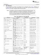
Table 5. Bill of Materials for LP8756xQ1EVM (continued)
Designator
Description
Manufacturer
Part Number
Qty.
J1A, J2A, J3A, J4
RES, 0, 5%, 0.063 W, 0402
Vishay-Dale
CRCW04020000Z0ED
0 - 4
R6, R19
RES, 0, 5%, 0.1 W, 0603
Vishay-Dale
CRCW06030000Z0EA
0
R7, R8, R9, R10, R11, R12, R13
RES, 1.8 k, 5%, 0.1 W, 0603
Vishay-Dale
CRCW06031K80JNEA
0
R23
RES, 50, 1%, 0.1 W, 0603
Vishay-Dale
CRCW060350R0FKEA
0
TP1, TP2, TP3, TP4, TP7
Header, 100mil, 2x1, Gold, TH
Samtec
TSW-102-07-G-S
0
X4, X6
Receptacle, 2.5mm, 3x2, Gold, SMT
TE Connectivity
6651712-1
0
5
Board Layout
This section describes the board layout of the LP8756xQ1EVM. See the
for
specific PCB layout recommendations.
The board is constructed on a 6-layer PCB. using 60-µm copper on top and bottom layers to reduce
resistance and improve heat transfer. Similar layout can be done as a 4-layer board but 6 layers were
chosen to improve grounding and reduce DC resistance.
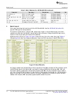
Board stack-up is shown in
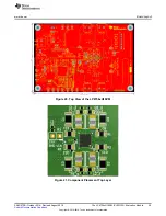
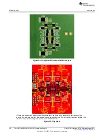
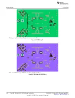
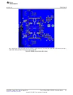
shows the top view of the entire board and
through
show the component placement, layout, and 3D view close to the LP8756 device.
Figure 19. Board Stack-Up
The design utilizes dual side placement of the components. This allows placement of the inductors next to
the LP8756xQ1 device for reducing SW node area for improved efficiency and reduced EMI. SW nets
have also snubber components to reduce SW pin spiking and EMI. The input capacitors can be placed
very close to the LP8756xQ1 device, to bottom side, to keep parasitic inductances low, and there is also
space for input filters for further EMI reduction. With these modifications, the EVMs can pass CISPR25
radiated and conducted EMI test without (optional) EMI shields H5 and H6.

