

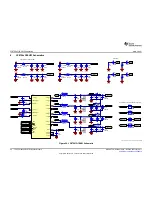


VUSB
15pF
C37
15pF
C38
GND
GND
XOU
T
X
IN
DHSDM
0.1µF
C44
0.1µF
C43
0.1µF
C45
0.1µF
C42
0.1µF
C41
GND
10µF
C40
JTAGSEL
48
TCK/SWCLK
56
TDI
51
TDO/TRACESWO
54
TMS/SWDIO
55
U2C
ATSAM3U2CA-AU
GNDBU
46
ADVREF
2
AD12BVREF
4
GNDANA
3
GND
35
GND
61
GND
89
GNDPLL
72
VDDOUT
52
VDDIN
53
VDDIO
60
VDDIO
88
VDDCORE
9
VDDCORE
34
VDDANA
1
VDDBU
45
VDDPLL
73
VDDCORE
59
VDDCORE
83
VDDCORE
87
VDDIO
36
VDDIO
22
U2D
ATSAM3U2CA-AU
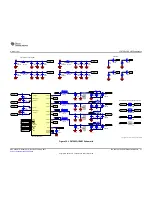
XOUT
XIN
GND
VUTMI
6.80k
R24
GND
10pF
C36
39.0
R26
39.0
R25
GND
DHSDP
DHSDM
VBG
GND
0.1µF
C51
GND
10µF
C49
HSI2C_SYS
SCL
SDA
PU_EN
HS_I2C
1.00k
R31
1.00k
R32
1µF
C61
GND
GND
10µF
C57
1.00
R29
0.1µF
C56
+3.3V
VUTMI
GND
10pF
C54
10µF
C55
DHSDP
VBUS_USB
0.1µF
C50
0.1µF
C52
0.1µF
C53
0.1µF
C48
GND
10µF
C47
TP22
PA0/PGMNCMD
26
PA1/PGMRDY
27
PA10/PGMD2
39
PA11/PGMD3
40
PA12/PGMD4
41
PA13/PGMD5
10
PA14/PGMD6
11
PA15/PGMD7
12
PA16/PGMD8
13
PA17/PGMD9
14
PA18/PGMD10
17
PA19/PGMD11
18
PA2/PGMNOE
28
PA20/PGMD12
19
PA21/PGMD13
20
PA22/PGMD14
5
PA23/PGMD15
21
PA24
23
PA25
24
PA26
25
PA27
96
PA28
84
PA29
85
PA3/PGMNVALID
29
PA30
6
PA31
86
PA4/PGMM0
30
PA5/PGMM1
31
PA6/PGMM2
32
PA7/PGMM3
33
PA8/PGMD0
37
PA9/PGMD1
38
PB0
90
PB1
91
PB10
70
PB11
93
PB12
94
PB13
95
PB14
69
PB15
16
PB16
15
PB17
68
PB18
67
PB19
66
PB2
92
PB20
65
PB21
64
PB22
63
PB23
62
PB24
58
PB3
7
PB4
8
PB5
97
PB6
98
PB7
99
PB8
100
PB9
71
U2A
ATSAM3U2CA-AU
DHSDP
76
DHSDM
77
FWUP
42
NRST
57
XOUT32
49
TST
44
ERASE
43
NRSTB
47
XIN32
50
XOUT
74
XIN
75
VBG
78
DFSDM
80
DFSDP
81
VDDUTMI
79
GNDUTMI
82
U2B
ATSAM3U2CA-AU
LDO1: 1.8 V (150 mA), VDDIO for SAM3U
LDO2: 3.3 V (300 mA), 3.3V generic supply
IN
1
NC
7
EN1
2
OUT2
9
EN2
3
DAP
11
POR
8
OUT1
10
SET
5
GND
6
CBYP
4
U3
LP3996SD-1833/NOPB
+3.3V
GND
GND
GND
VUSB
GND
GND
0.01µF
C62
1µF
C60
1µF
C59
1µF
C58
470k
R30
GND
L8
LB2012T100KR
1
2
3
J10
HTSW-103-07-G-S
VIO +3.3V
+3.3V
VIO
VDDOUT
VDDOUT
CLKINB2B
1V8out
D2
BAT42WS-7-F
68.0k
R27
VIO
0.1µF
C39
+3.3V
Diode for clamping
voltage to IO level
(1.8V/3.3V).
DFSDM
DFSDP
12MHz
1
2
Y1
GND
0.1µF
C46
GND
GND
8
9
VBUS
1
GND
5
6
7
D-
2
D+
3
ID
4
J9
1734035-2
GND
33.0k
R28
GND
VBUS_USB
SCL
HSI2C_SYS
HSI2C_SYS
SDA
HSI2C_SYS
PU_EN
VCC1V8
INTB2B
NRSTB2B
EN1B2B
EN2B2B
EN3B2B
PGOODB2B
I2C Pull-up
I/O supply
Copyright © 2016, Texas Instruments Incorporated
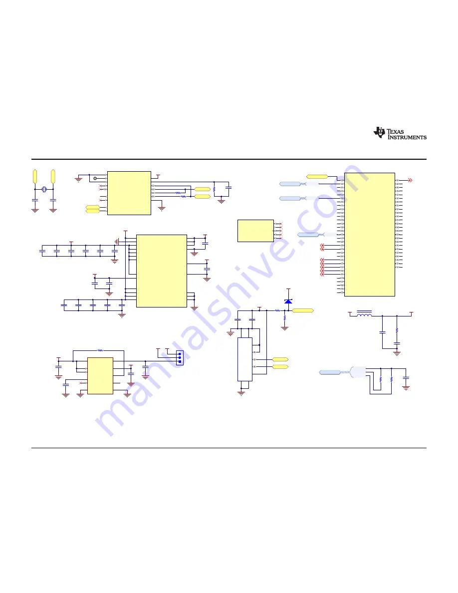
LP8756xQ1EVM Schematics
www.ti.com
36
SNVU472A – October 2016 – Revised February 2017
Submit Documentation Feedback
Copyright © 2016–2017, Texas Instruments Incorporated
The LP8756xQ1EVM Evaluation Module
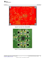
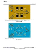
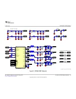
Figure 35. EVM I
2
C Interface


