MSP430FG47x
MIXED SIGNAL MICROCONTROLLER
SLAS580D -- OCTOBER 2008 -- REVISED MARCH 2011
16
POST OFFICE BOX 655303
DALLAS, TEXAS 75265
peripherals
Peripherals are connected to the CPU through data, address, and control buses and can be handled using all
instructions. For complete module descriptions, see the
MSP430x4xx Family User’s Guide
, literature number
SLAU056.
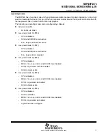
oscillator and system clock
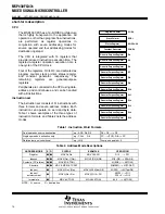
The clock system in the MSP430FG47x is supported by the FLL+ module, which includes support for a
32768-Hz watch crystal oscillator, an internal digitally-controlled oscillator (DCO), and a 8-MHz high-frequency
crystal oscillator (XT1), plus a 8-MHz high-frequency crystal oscillator (XT2). The FLL+ clock module is
designed to meet the requirements of both low system cost and low power consumption. The FLL+ features
digital frequency locked loop (FLL) hardware that, in conjunction with a digital modulator, stabilizes the DCO
frequency to a programmable multiple of the watch crystal frequency. The internal DCO provides a fast turn-on
clock source and stabilizes in less than 6
s. The FLL+ module provides the following clock signals:
D
Auxiliary clock (ACLK), sourced from a 32768-Hz watch crystal or a high-frequency crystal
D
Main clock (MCLK), the system clock used by the CPU
D
Sub-Main clock (SMCLK), the sub-system clock used by the peripheral modules
D
ACLK/n, the buffered output of ACLK, ACLK/2, ACLK/4, or ACLK/8
brownout, supply voltage supervisor
The brownout circuit is implemented to provide the proper internal reset signal to the device during power on
and power off. The supply voltage supervisor (SVS) circuitry detects if the supply voltage drops below a user
selectable level and supports both supply voltage supervision (the device is automatically reset) and supply
voltage monitoring (SVM, the device is not automatically reset).
The CPU begins code execution after the brownout circuit releases the device reset. However, V
CC
may not
have ramped to V
CC(min)
at that time. The user must ensure the default FLL+ settings are not changed until V
CC
reaches V
CC(min)
. If desired, the SVS circuit can be used to determine when V
CC
reaches V
CC(min)
.
digital I/O
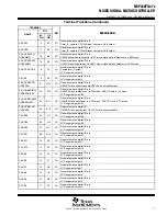
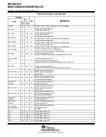
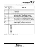
There are six 8-bit I/O ports implemented, ports P1 through P6.
D
All individual I/O bits are independently programmable.
D
Any combination of input, output, and interrupt conditions is possible.
D
Edge-selectable interrupt input capability for all the eight bits of ports P1 and P2.
D
Read/write access to port-control registers is supported by all instructions.
Summary of Contents for MSP430FG47x
Page 91: ......

