MSP430FG47x
MIXED SIGNAL MICROCONTROLLER
SLAS580D -- OCTOBER 2008 -- REVISED MARCH 2011
17
POST OFFICE BOX 655303
DALLAS, TEXAS 75265
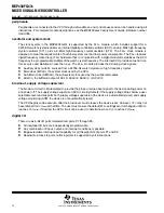
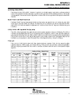
watchdog timer (WDT+)
The primary function of the WDT+ module is to perform a controlled system restart after a software problem
occurs. If the selected time interval expires, a system reset is generated. If the watchdog function is not needed
in an application, the module can be configured as an interval timer and can generate interrupts at selected time
intervals.
Basic Timer1 and Real-Time Clock
The Basic Timer1 has two independent 8-bit timers that can be cascaded to form a 16-bit timer/counter. Both
timers can be read and written by software. The Basic Timer1 is extended to provide an integrated real-time
clock (RTC). An internal calendar compensates for month with less than 31 days and includes leap year
correction.
LCD_A driver with regulated charge pump
The LCD_A driver generates the segment and common signals required to drive an LCD display. The LCD_A
controller has dedicated data memory to hold segment drive information. Common and segment signals are
generated as defined by the mode. Static, 2-MUX, 3-MUX, and 4-MUX LCDs are supported by this peripheral.
The module can provide a LCD voltage independent of the supply voltage via an integrated charge pump.
Furthermore, it is possible to control the level of the LCD voltage and, thus, contrast in software.
Timer_A3
Timer_A3 is a 16-bit timer/counter with three capture/compare registers. Timer_A3 can support multiple
capture/compares, PWM outputs, and interval timing. Timer_A3 also has extensive interrupt capabilities.
Interrupts may be generated from the counter on overflow conditions and from each of the capture/compare
registers.
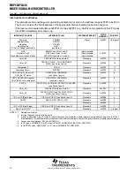
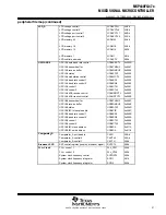
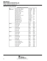
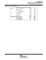
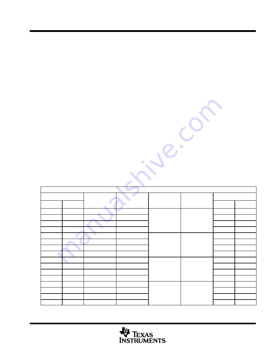
TIMER_A3 SIGNAL CONNECTIONS
INPUT PIN NUMBER
DEVICE INPUT
MODULE INPUT
MODULE
MODULE
OUTPUT
OUTPUT PIN NUMBER
PN
ZQW
DEVICE INPUT
SIGNAL
MODULE INPUT
NAME
MODULE
BLOCK
OUTPUT
SIGNAL
PN
ZQW
P1.5 -- 51
F11
TACLK
TACLK
ACLK
ACLK
Timer
NA
SMCLK
SMCLK
Timer
NA
P1.5 -- 51
F11
TAINCLK
INCLK
P1.0 -- 58
C11
TA0
CCI0A
P1.0 -- 58
C11
P1.1 -- 57
C12
TA0
CCI0B
CCR0
TA0
P1.1 -- 57
C12
DV
SS
GND
CCR0
TA0
DV
CC
V
CC
P1.2 -- 56
D11
TA1
CCI1A
P1.2 -- 56
D11
CAOUT (internal)
CCI1B
CCR1
TA1
DV
SS
GND
CCR1
TA1
DV
CC
V
CC
P2.0 -- 4
C2
TA2
CCI2A
P2.0 -- 4
C2
ACLK (internal)
CCI2B
CCR2
TA2
DV
SS
GND
CCR2
TA2
DV
CC
V
CC
Summary of Contents for MSP430FG47x
Page 91: ......

