background image

Description of Switches and Buttons

2-7

Detailed Description of the EVM

2.5

Description of Switches and Buttons

2.5.1

S/PDIF Input Selector Switch (S100)

S100 switches between optical and coaxial S/PDIF input. When the lever is
pressed in the direction of J101, the optical S/PDIF input is selected. When the
lever is pressed in the direction of J100, the coaxial S/PDIF input is selected.

2.5.2

Bypass Digital Audio Processor Switch (S320)

When the lever is pressed in the direction of S341, the DAP is bypassed. When
the lever is pressed in the direction of U360 (TAS3002), the DAP is in the signal
path. Below S320 is a label (DAP ON), which indicates the position of the lever
for the DAP inserted in signal path.

Warning 

Bypassing the DAP is equal to maximum output power (attenuation = 0 dB). This
might be loud and could possible damage your loudspeaker and hearing.

2.5.3

Reset Board Button (S620)

This is the master RESET for the EVM board. While this button is held down,
the DIR1703, TAS3002, TAS5001, and TAS5122DCA are held RESET and
latching errors are cleared. Note that while the RESET button is held down,
the No S/PDIF LED lights up, even if a valid S/PDIF input signal is present,
because the DIR1703 S/PDIF receiver is held RESET.

2.5.4

Mute Button (S240)

The output stage is muted (not switching) while this button is held down and
unmutes when it is released.

2.5.5

Volume Control (S340 and S341)

S341 and S340: Volume control of TAS3002 DAP. Press and hold the S341
button to decrease output power level. Press and hold the S340 button to
increase output power level.

Note:

Change of listening level is slow. It takes approximately 25 seconds to
change attenuation from –70 dB to 0 dB.

The TAS3002 device implements a soft volume control. This feature allows a
change from one volume level to another over the entire range of volume
control (+18 dB to mute). Above 0 dB, there is risk of signal clipping. Distortion
of output signals is the result of signal clipping.

Note:

Significant signal clipping might result in activation of the overcurrent
protection system.

Summary of Contents for TAS5001-5122C2EVM

Page 1: ...June 2004 DAV Digital Audio Speaker User s Guide SLEU055...

Page 2: ...ute a license from TI to use such products or services or a warranty or endorsement thereof Use of such information may require a license from a third party under the patents or other intellectual pro...

Page 3: ...handling or use of the goods Please be aware that the products received may not be regulatory compliant or agency certified FCC UL CE etc Due to the open construction of the product it is the user s r...

Page 4: ...M output If there is uncertainty as to the load specification please contact a TI field representative During normal operation some circuit components may have case temperatures greater than 60 C The...

Page 5: ...2 Detailed Description of the EVM Board Chapter 3 EVM Board Operation Chapter 4 Hints for Measurements of Performance Information About Cautions and Warnings This book may contain cautions and warning...

Page 6: ...DBVR SCES219 SN74LV21APWR SCES340 Additional TAS5001 5122C2EVM Documentation DCT Software and User s Guide for Controlling the TAS3002 TAS5001 5122C2EVM Application Report SLEA035 Data Manuals FCC War...

Page 7: ...ctor 2 6 2 5 Description of Switches and Buttons 2 7 2 5 1 S PDIF Input Selector Switch S100 2 7 2 5 2 Bypass Digital Audio Processor Switch S320 2 7 2 5 3 Reset Board Button S620 2 7 2 5 4 Mute Butto...

Page 8: ...2 4 2 5 Pin Numbers at the Parallel Port I2C Interface I2C J300 2 5 2 6 Pin Numbers at PSU Connector Top View 2 6 3 1 Recommended Power Up and Power Down Sequence 3 2 3 2 EVM Board Connected to S PDIF...

Page 9: ...e TAS5010 PCM PWM modulator The maximum sample rate for the TAS5010 is 192 kHz Together the TAS5001 and one TAS5122DCA provide the complete PurePath DigitalTM conversion of a 3 3 V digital audio input...

Page 10: ...CESSOR TAS5122DCA DIGITAL AUDIO PWM POWER OUTPUT STAGE I2C BUS I2S BUS I2S BUS PC SOFTWARE OPTICAL INPUT COAXIAL INPUT I2S INPUT 32 kHz 96 kHz 32 kHz 192 kHz ANALOG INPUT ANALOG OUTPUT VOLUME CONTROL...

Page 11: ...s and with two push buttons on the EVM board During power up the TAS3002 settings and coefficients are loaded from an external serial EEPROM The TAS3002 coefficients control all features in the DAP Cu...

Page 12: ...1 4...

Page 13: ...egards to board layout jumpers switches buttons and connectors Topic Page 2 1 Board Overview 2 2 2 2 Description of Jumper Settings 2 3 2 3 Default Jumper Positioins 2 4 2 4 Description of Connectors...

Page 14: ...Switch between Optical and Coaxial input ACTIVE BYPASSED EQUALIZER ENABLE EQ DISABLE EQ ENABLE SAMPLE RATE CONTROL S PDIF ERROR ENABLE Coaxial Optical LED223 LED222 LED221 LED220 POWER NO S PDIF TEMP...

Page 15: ...UNLOCK DIR1703 ADFLG The DIR1703 UNLOCK signal is high until the PLL in DIR1703 detects and locks on an incoming digital signal The ADFLG signal is high when the S PDIF data does not include a PCM aud...

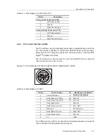
Page 16: ...ghest sampling rate supported for this input is 96 kHz 2 4 2 S PDIF Optical J101 The Toslink connector can be connected to a digital S PDIF signal through an optical cable The highest sampling rate su...

Page 17: ...ware saved on the PurePath DigitalTM amplifier CD ROM The PC interface can also be used to control the TAS3002 from an external microcontroller of your own choice Figure 2 5 Pin Numbers at the Paralle...

Page 18: ...egative output terminal J580 Right speaker positive output terminal J581 Right speaker negative output terminal Caution Both positive and negative speaker outputs are floating and may NOT be connected...

Page 19: ...M board While this button is held down the DIR1703 TAS3002 TAS5001 and TAS5122DCA are held RESET and latching errors are cleared Note that while the RESET button is held down the No S PDIF LED lights...

Page 20: ...e TAS5122 junction has reached the warning level This is step one of the two step thermal protection system implemented in the TAS5122 device The temperature warning is an indication only the operatio...

Page 21: ...board operation Topic Page 3 1 Power Supply 3 2 3 2 Setup the TAS5001 5122C2EVM With the S PDIF Input 3 3 3 3 Setup the TAS5001 5122C2EVM With the Analog Line Input 3 4 3 4 Interfacing the Analog Lin...

Page 22: ...ed power supply is not allowed to be below 15 V The maximum supply voltage depends of the speaker load resistance Check the recommended maximum supply voltage in the TAS5122DCA data sheet SLES088 Tabl...

Page 23: ...ed a cable for PC communication are initially connected to the EVM board 3 The TAS5001 5122C2EVM can be powered with either one or two power supplies see the Power Supply section Power supplies are in...

Page 24: ...NLOCK warning from S PDIF receiver JMP130 shunts pin 2 and 3 Connect TAS5001 5122C2EVM board and PC with the attached cable Connect analog source to analog input J160 Power up the TAS5001 5122C2EVM bo...

Page 25: ...ments Specifications for the AES17 filter are described in the AES Standard Method For Digital Audio Engineering Measurement of Digital Audio Equipment the AES17 standard is available from the Audio E...

Page 26: ...4 2...

Page 27: ...Mouser Electronics Authorized Distributor Click to View Pricing Inventory Delivery Lifecycle Information Texas Instruments TAS5001 5122C2EVM...

Reviews: