background image

1

2

3

4

5

1

0

1

1

1

1

0

0

0

0

CLK

OE(ED2)

LE(ED1)

1

2

3

0

4

6

7

5

0

1

off

on

off

on

off

on

off

on

off

on

Don't care

CLK

OE(ED2)

LE(ED1)

SDI

OUT0

OUT1

OUT2

OUT3

OUT7

SDO

TLC5916, TLC5917

www.ti.com

SLVS695D – JUNE 2007 – REVISED JANUARY 2015

Device Functional Modes (continued)

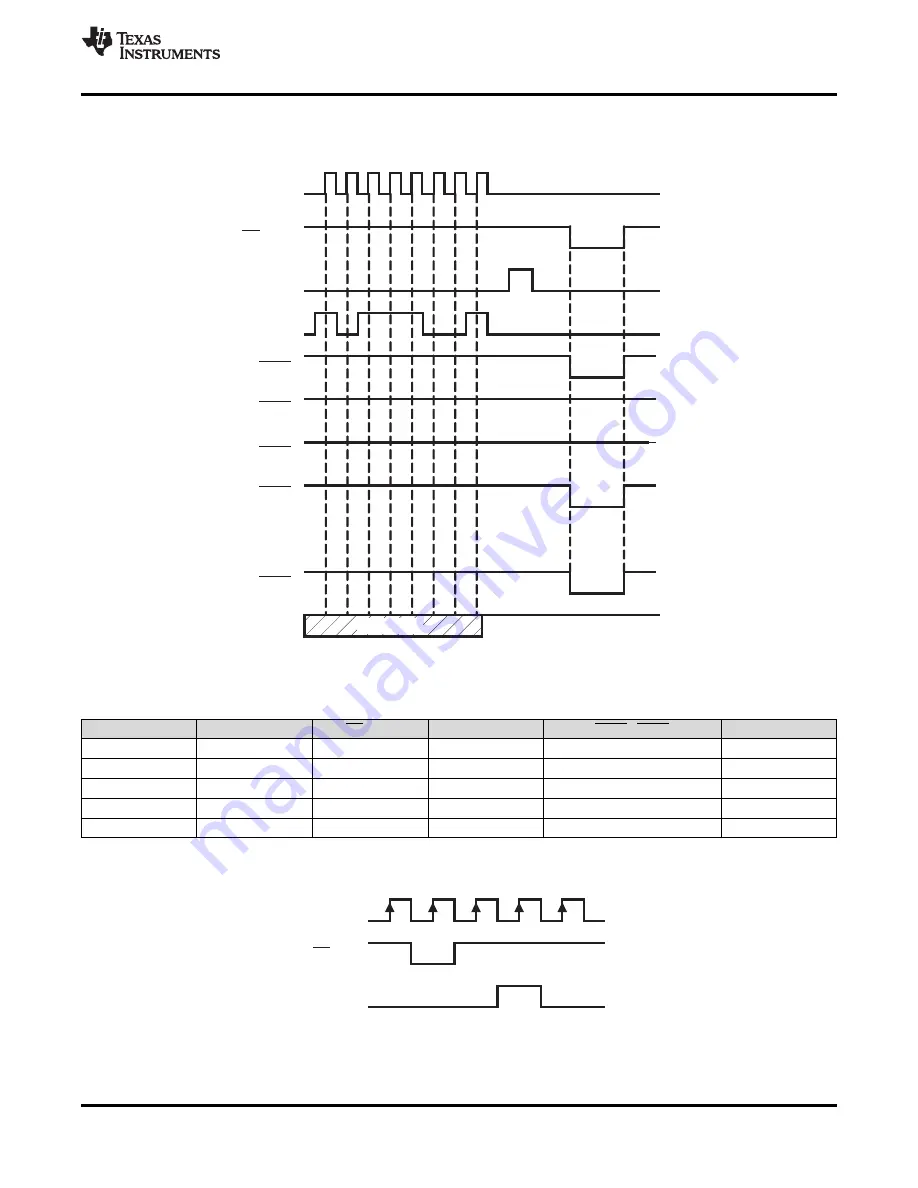
Figure 11. Normal Mode

Table 4. Truth Table in Normal Mode

CLK

LE(ED1)

OE(ED2)

SDI

OUT0...OUT7

SDO

H

L

Dn

Dn...Dn – 7

Dn – 7

L

L

Dn + 1

No change

Dn – 6

H

L

Dn + 2

Dn + 2...Dn – 5

Dn – 5

X

L

Dn + 3

Dn + 2...Dn – 5

Dn – 5

X

H

Dn + 3

Off

Dn – 5

The signal sequence shown in

Figure 12

makes the TLC591x enter Current Adjust and Error Detection Mode.

Figure 12. Switching to Special Mode

In the Current Adjust Mode, sending the positive pulse of LE(ED1), the content of the shift register (a current
adjust code) is written to the 8-bit configuration latch (see

Figure 13

).

Copyright © 2007–2015, Texas Instruments Incorporated

Submit Documentation Feedback

17

Product Folder Links:

TLC5916 TLC5917

Summary of Contents for TLC5916

Page 1: ...n to sink 256 Step Programmable Global Current Gain various currents which provides optional Excellent Output Current Accuracy implementation of multi color LEDs An additional Between Channels 3 Maximum advantage of the independent outputs is the ability to Between ICs 6 Maximum leave unused channels floating The flexibility of the TLC591x LED drivers is ideal for applications such as Fast Respons...

Page 2: ...ackaging and Orderable 8 Parameter Measurement Information 10 Information 29 4 Revision History NOTE Page numbers for previous revisions may differ from page numbers in the current version Changes from Revision C February 2011 to Revision D Page Added Pin Configuration and Functions section ESD Ratings table Feature Description section Device Functional Modes Application and Implementation section...

Page 3: ...atch when LE ED1 is high The data is latched LE ED1 4 I when LE ED1 goes low Also a control signal input for an Error Detection Mode and Current Adjust Mode see Timing Diagram LE ED1 has an internal pulldown Output enable When OE ED2 is active low the output drivers are enabled when OE ED2 is high all output drivers are turned OFF blanked Also a control signal input for OE ED2 13 I an Error Detect...

Page 4: ...control process 2 JEDEC document JEP157 states that 250 V CDM allows safe manufacturing with a standard ESD control process 7 3 Recommended Operating Conditions MIN MAX UNIT VDD Supply voltage 3 5 5 V VO Supply voltage to output pins OUT0 OUT7 20 V VO 0 6 V 3 IO Output current DC test circuit mA VO 1 V 120 IOH High level output current source SDO shorted to GND 1 mA IOL Low level output current si...

Page 5: ...die 2 6 IO 2 TJ 25 C Output current skew channel to IOL 52 mA VO 0 8 V Rext 360 Ω 1 5 3 channel TJ 25 C VO 1 V to 3 V IO 26 mA 0 1 IOUT vs Output current vs V VDD 3 0 V to 5 5 V VOUT output voltage regulation 1 IO 26 mA 120 mA Pullup resistance OE ED2 500 kΩ Pulldown resistance LE ED1 500 kΩ Tsd Overtemperature shutdown 2 150 175 200 C Thys Restart temperature hysteresis 2 15 C Threshold current f...

Page 6: ... die 2 6 IO 2 TJ 25 C Output current skew channel to IOL 52 mA VO 0 8 V Rext 360 Ω 1 5 3 channel TJ 25 C VO 1 V to 3 V IO 26 mA 0 1 IOUT vs Output current vs V VDD 3 0 V to 5 5 V VOUT output voltage regulation 1 IO 26 mA 120 mA Pullup resistance OE ED2 500 kΩ Pulldown resistance LE ED1 500 kΩ Tsd Overtemperature shutdown 2 150 175 200 C Thys Restart temperature hysteresis 2 15 C Threshold current ...

Page 7: ...ror Detection Mode 2 μs Rext 360 Ω VL 4 V RL 44 Ω CL 10 pF th ED1 ED2 Hold time LE ED1 and OE ED2 10 ns CG 0 992 th D Hold time SDI 2 ns tsu D ED1 Setup time SDI LE ED1 3 ns tsu ED2 Setup time OE ED2 8 5 ns th L Hold time LE ED1 Normal Mode 15 ns tsu L Setup time LE ED1 Normal Mode 15 ns tr Rise time CLK 2 500 ns tf Fall time CLK 2 500 ns tor Rise time outputs off 40 85 105 ns tor Rise time output...

Page 8: ...r Detection Mode 2 μs Rext 360 Ω VL 4 V RL 44 Ω CL 10 pF th D ED1 ED2 Hold time SDI LE ED1 and OE ED2 10 ns CG 0 992 th D Hold time SDI 2 ns tsu D ED1 Setup time SDI LE ED1 3 ns tsu ED2 Setup time OE ED2 8 5 ns th L Hold time LE ED1 Normal Mode 15 ns tsu L Setup time LE ED1 Normal Mode 15 ns tr Rise time CLK 2 500 ns tf Fall time CLK 2 500 ns tor Rise time outputs off 40 85 105 ns tor Rise time ou...

Page 9: ...SDI Normal Mode 3 ns th D Hold time for SDI Normal Mode 2 ns tsu L Setup time for LE ED1 Normal Mode 15 ns th L Hold time for LE ED1 Normal Mode 15 ns tw CLK CLK pulse duration Error Detection Mode 20 ns tw ED2 OE ED2 pulse duration Error Detection Mode 2000 ns tsu ED1 Setup time for LE ED1 Error Detection Mode 4 ns th ED1 Hold time for LE ED1 Error Detection Mode 10 ns tsu ED2 Setup time for OE E...

Page 10: ...VDD OE ED2 CLK LE ED1 SDI R EXT GND SDO OUT7 OUT0 TLC5916 TLC5917 SLVS695D JUNE 2007 REVISED JANUARY 2015 www ti com 8 Parameter Measurement Information Figure 5 Test Circuit for Electrical Characteristics Figure 6 Test Circuit for Switching Characteristics 10 Submit Documentation Feedback Copyright 2007 2015 Texas Instruments Incorporated Product Folder Links TLC5916 TLC5917 ...

Page 11: ...tsu D th D 50 tw OE tPHL3 tof tor Output off tPLH3 50 20 80 OE ED2 OUTn 50 80 50 20 HIGH TLC5916 TLC5917 www ti com SLVS695D JUNE 2007 REVISED JANUARY 2015 Parameter Measurement Information continued Figure 7 Normal Mode Timing Waveforms Copyright 2007 2015 Texas Instruments Incorporated Submit Documentation Feedback 11 Product Folder Links TLC5916 TLC5917 ...

Page 12: ...695D JUNE 2007 REVISED JANUARY 2015 www ti com Parameter Measurement Information continued Figure 8 Switching to Special Mode Timing Waveforms Figure 9 Reading Error Status Code Timing Waveforms 12 Submit Documentation Feedback Copyright 2007 2015 Texas Instruments Incorporated Product Folder Links TLC5916 TLC5917 ...

Page 13: ...one clock wide pulse appears on OE ED2 the device enters the Mode Switching phase At this time the voltage level on LE ED1 determines which mode the TLC591x switches to In the Normal Mode phase the serial data can be transferred into TLC591x through the pin SDI shifted in the shift register and transferred out via the pin SDO LE ED1 can latch the serial data in the shift register to the output lat...

Page 14: ...be on Table 1 Open Circuit Detection CONDITION OF OUTPUT STATE OF OUTPUT PORT ERROR STATUS CODE MEANING CURRENT Off IOUT 0 mA 0 Detection not possible IOUT IOUT Th 1 0 Open circuit On IOUT IOUT Th 1 Channel n error status bit 1 Normal 1 IOUT Th 0 5 IOUT target typical 9 3 2 Short Circuit Detection Principle TLC5917 Only The LED short circuit detection compares the effective voltage level VOUT with...

Page 15: ...egister of every channel After shutdown the channels automatically restart after cooling down if the control signal output latch remains on The stored error status is not reset after cooling down and can be read out as the error status code in the Special Mode When one of the channel specific sensors reaches trip temperature only the affected output channel is shut down and the error status is sto...

Page 16: ...DI shifted in the shift register and transferred out via the pin SDO LE ED1 can latch the serial data in the shift register to the output latch OE ED2 enables the output drivers to sink current In the Special Mode phase the low voltage level signal on OE ED2 can enable output channels and detect the status of the output current to determine if the driving current level is sufficient The detected E...

Page 17: ...T7 SDO H L Dn Dn Dn 7 Dn 7 L L Dn 1 No change Dn 6 H L Dn 2 Dn 2 Dn 5 Dn 5 X L Dn 3 Dn 2 Dn 5 Dn 5 X H Dn 3 Off Dn 5 The signal sequence shown in Figure 12 makes the TLC591x enter Current Adjust and Error Detection Mode Figure 12 Switching to Special Mode In the Current Adjust Mode sending the positive pulse of LE ED1 the content of the shift register a current adjust code is written to the 8 bit ...

Page 18: ...uence shown in Figure 15 makes TLC591x resume the Normal Mode Switching to Normal Mode resets all internal Error Status registers OE ED2 always enables the output port whether the TLC591x enters Current Adjust Mode or not Figure 15 Switching to Normal Mode 9 4 1 Operation Mode Switching To switch between its two modes TLC591x monitors the signal OE ED2 When an one clock wide pulse of OE ED2 appear...

Page 19: ... TLC591x to switch the operation mode However as long as LE ED1 is high in the Mode Switching phase TLC591x remains in the Normal Mode as if no mode switching occurred 9 4 1 2 Special Mode Phase In the Special Mode as long as OE ED2 is not low the serial data is shifted to the Shift Register via SDI and shifted out via SDO as in the Normal Mode However there are two differences between the Special...

Page 20: ...ED1 latches the serial data in the Shift Register to the Configuration Latch instead of the Output Latch The latched serial data is used as the Configuration Code The code is stored until power off or the Configuration Latch is rewritten As shown in Figure 18 the timing for writing the Configuration Code is the same as the timing in the Normal Mode to latching output channel data Both the Configur...

Page 21: ...rent Iout at each output port Users can follow the below formulas to calculate the target output current IOUT target in the saturation region In the equations Rext is the resistance of the external resistor connected between the R EXT terminal and ground and VR EXT is the voltage of R EXT which is controlled by the programmable voltage gain VG VG is defined by the Configuration Code VR EXT 1 26 V ...

Page 22: ...LC5917 720Ω GND OE SDO R EXT VDD LE CLK SDI OUT0 OUT7 TLC5917 Read Back TLC5916 TLC5917 SLVS695D JUNE 2007 REVISED JANUARY 2015 www ti com Application Information continued 10 1 3 Cascading Implementation of TLC591x Device Figure 20 Cascading Implementation of TLC591x Device 22 Submit Documentation Feedback Copyright 2007 2015 Texas Instruments Incorporated Product Folder Links TLC5916 TLC5917 ...

Page 23: ...and two sub bands Low voltage sub band HC 0 VG 1 4 127 256 linearly divided into 64 steps High voltage sub band HC 1 VG 1 2 127 128 linearly divided into 64 steps CM In addition to determining the ratio IOUT target Iref CM limits the output current range High Current Multiplier CM 1 IOUT target Iref 15 suitable for output current range IOUT 10 mA to 120 mA Low Current Multiplier CM 0 IOUT target I...

Page 24: ...High Current Multiplier Configuration Code CM HC CC 0 5 in Binary Format Current Gain CG TLC5916 TLC5917 SLVS695D JUNE 2007 REVISED JANUARY 2015 www ti com Figure 21 Current Gain vs Configuration Code 10 2 Typical Application Figure 22 shows implementation of a single TLC591x device Figure 20 shows a cascaded driver implementation Figure 22 Single Implementation of TLC591x Device 24 Submit Documen...

Page 25: ... resistance PD_TOT is the total power dissipation in the IC 12 PD_TOT PD_CS IDD VDD where PD_CSis the power dissipation in the LED current sinks IDD is the IC supply current VDD is the IC supply voltage 13 PD_CS IO VO nCH where IO is the LED current VO is the voltage at the output pin nCH is the number of LED strings 14 VO VLED nLED VF where VLED is the voltage applied to the LED string nLED is th...

Page 26: ...ure is kept below 150 C NOTE This design example assumes that all channels have the same electrical parameters nLED IO VF VLED If the parameters are unique for each channel then the power dissipation must be calculated for each current sink separately Then each result must be added together to calculate the total power dissipation in the current sinks 10 2 3 Application Curve Figure 23 Output Curr...

Page 27: ...e LEDs 12 Layout 12 1 Layout Guidelines The traces that carry current from the LED cathodes to the OUTx pins must be wide enough to support the default current up to 120 mA The SDI CLK LE ED1 OE ED2 and SDO pins are to be connected to the microcontroller There are several ways to achieve this including the following methods Traces may be routed underneath the package on the top layer The signal ma...

Page 28: ... VIA to GND To µC To µC VDD To µC To µC To µC TLC5916 TLC5917 SLVS695D JUNE 2007 REVISED JANUARY 2015 www ti com Layout Example continued Figure 25 D Package Layout 28 Submit Documentation Feedback Copyright 2007 2015 Texas Instruments Incorporated Product Folder Links TLC5916 TLC5917 ...

Page 29: ...ostatic Discharge Caution These devices have limited built in ESD protection The leads should be shorted together or the device placed in conductive foam during storage or handling to prevent electrostatic damage to the MOS gates 13 4 Glossary SLYZ022 TI Glossary This glossary lists and explains terms acronyms and definitions 14 Mechanical Packaging and Orderable Information The following pages in...

Page 30: ... 2000 Green RoHS no Sb Br NIPDAU Level 1 260C UNLIM 40 to 125 Y5916 TLC5916IPWRG4 ACTIVE TSSOP PW 16 2000 Green RoHS no Sb Br NIPDAU Level 1 260C UNLIM 40 to 125 Y5916 TLC5917ID ACTIVE SOIC D 16 40 Green RoHS no Sb Br NIPDAU Level 1 260C UNLIM 40 to 125 TLC5917I TLC5917IDR ACTIVE SOIC D 16 2500 Green RoHS no Sb Br NIPDAU Level 1 260C UNLIM 40 to 125 TLC5917I TLC5917IDRG4 ACTIVE SOIC D 16 2500 Gree...

Page 31: ...or the environmental category on the device 5 Multiple Device Markings will be inside parentheses Only one Device Marking contained in parentheses and separated by a will appear on a device If a line is indented then it is a continuation of the previous line and the two combined represent the entire Device Marking for that device 6 Lead Ball Finish Orderable Devices may have multiple material fini...

Page 32: ... P1 mm W mm Pin1 Quadrant TLC5916IDR SOIC D 16 2500 330 0 16 4 6 5 10 3 2 1 8 0 16 0 Q1 TLC5916IPWR TSSOP PW 16 2000 330 0 12 4 6 9 5 6 1 6 8 0 12 0 Q1 TLC5917IDR SOIC D 16 2500 330 0 16 4 6 5 10 3 2 1 8 0 16 0 Q1 TLC5917IPWR TSSOP PW 16 2000 330 0 12 4 6 9 5 6 1 6 8 0 12 0 Q1 PACKAGE MATERIALS INFORMATION www ti com 1 Oct 2014 Pack Materials Page 1 ...

Page 33: ...gth mm Width mm Height mm TLC5916IDR SOIC D 16 2500 333 2 345 9 28 6 TLC5916IPWR TSSOP PW 16 2000 367 0 367 0 35 0 TLC5917IDR SOIC D 16 2500 333 2 345 9 28 6 TLC5917IPWR TSSOP PW 16 2000 367 0 367 0 35 0 PACKAGE MATERIALS INFORMATION www ti com 1 Oct 2014 Pack Materials Page 2 ...

Page 34: ......

Page 35: ......

Page 36: ...r dimensions are in millimeters Any dimensions in parenthesis are for reference only Dimensioning and tolerancing per ASME Y14 5M 2 This drawing is subject to change without notice 3 This dimension does not include mold flash protrusions or gate burrs Mold flash protrusions or gate burrs shall not exceed 0 15 mm per side 4 This dimension does not include interlead flash Interlead flash shall not e...

Page 37: ...ed 6 Publication IPC 7351 may have alternate designs 7 Solder mask tolerances between and around signal pads can vary based on board fabrication site LAND PATTERN EXAMPLE EXPOSED METAL SHOWN SCALE 10X SYMM SYMM 1 8 9 16 15 000 METAL SOLDER MASK OPENING METAL UNDER SOLDER MASK SOLDER MASK OPENING EXPOSED METAL EXPOSED METAL SOLDER MASK DETAILS NON SOLDER MASK DEFINED PREFERRED SOLDER MASK DEFINED ...

Page 38: ...4 A 02 2017 NOTES continued 8 Laser cutting apertures with trapezoidal walls and rounded corners may offer better paste release IPC 7525 may have alternate design recommendations 9 Board assembly site may have different recommendations for stencil design SOLDER PASTE EXAMPLE BASED ON 0 125 mm THICK STENCIL SCALE 10X SYMM SYMM 1 8 9 16 ...

Page 39: ......

Page 40: ...se resources are subject to change without notice TI grants you permission to use these resources only for development of an application that uses the TI products described in the resource Other reproduction and display of these resources is prohibited No license is granted to any other TI intellectual property right or to any third party intellectual property right TI disclaims responsibility for...

Reviews: