background image

4.9.3.2

EQ Filters

4.9.3.3

Analog Simulation Filters

TLV320AIC3107EVM Software

www.ti.com

EQ, or parametric, filters can be designed on this tab (see

Figure 21

). Enter a gain, bandwidth, and a

center frequency (Fc). Either bandpass (positive gain) or band-reject (negative gain) filters can be created

Figure 21. EQ Filters

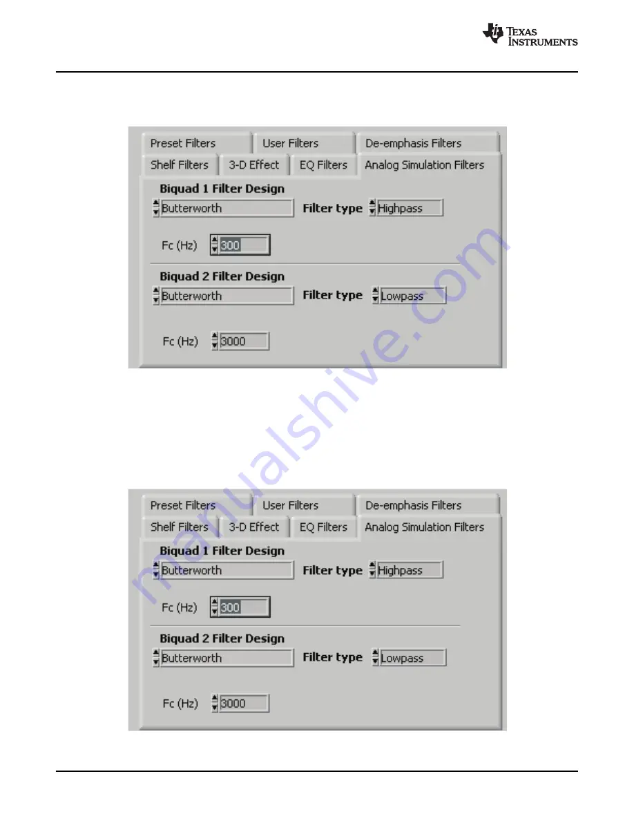
Biquads are good at simulating analog filter designs. For each biquad section on this tab, enter the
desired analog filter type to simulate (Butterworth, Chebyshev, Inverse Chebyshev, Elliptic, or Bessel).
Parameter entry boxes appropriate to the filter type are shown (ripple, for example, with Chebyshev filters,
etc.). Enter the desired design parameters, and the response is shown (

Figure 22

).

Figure 22. Analog Simulation Filters

TLV320AIC3107EVM-K

24

SLAU261 – November 2008

Submit Documentation Feedback

Summary of Contents for TLV320AIC3107

Page 1: ...able through the Texas Instruments Web site at www ti com EVM Compatible Device Data Sheets Device Literature Number TLV320AIC3107 SLOS545 TAS1020B SLES025 REG1117 3 3 SBVS001 TPS767D318 SLVS209 SN74LVC125A SCAS290 SN74LVC1G125 SCES223 SN74LVC1G07 SCES296 Contents 1 EVM Overview 3 2 EVM Description and Basics 3 3 TLV320AIC3107EVM K Setup and Installation 7 4 TLV320AIC3107EVM Software 8 Appendix A ...

Page 2: ... Tab 29 29 Class D Output Tab 30 30 Command Line Interface Tab 31 31 File Menu 32 C 1 Assembly layer 38 C 2 Top Layer 38 C 3 Layer 3 39 C 4 Layer 4 39 C 5 Bottom Layer 40 List of Tables 1 USB MODEVM SW2 Settings 5 2 List of Stand alone Jumpers 5 3 Switch SW1 Configurations 6 4 Switch SW2 Configurations 6 5 Switch SW3 Configurations 6 A 1 Analog Input Output Connectors 33 A 2 Block A and Block B Di...

Page 3: ...ts the TI Modular EVM format The TLV320AIC3107EVM K is a complete evaluation demonstration kit which includes a USB based motherboard called the USB MODEVM Interface board and evaluation software for use with a PC running the Microsoft Windows operating systems The USB connection from the PC provides power control and streaming audio data to the EVM for reduced setup and configuration The EVM also...

Page 4: ...ing the connecting pins The two boards can only be connected in one way It is suggested to first align with the 10 pin connectors J3 on the TLV320AIC3107EVM and J18A on the USB MODEVM and then gently push all the connectors together until the boards are seated In the factory configuration the board is ready to use with the TLV320AIC3107EVM To view all the functions and configuration options availa...

Page 5: ...eset Signal comes from USB MODEVM J15 8 EXT MCK External MCLK Selection ON MCLK Signal is provided from USB MODEVM J10 OFF MCLK Signal comes from either selection of SW2 5 Table 2 provides a list of jumpers found on the EVM and their factory default conditions Table 2 List of Stand alone Jumpers Jumper Jumper Default Number Type Position Jumper Description W1 2 pin soldered AVDD_ADC power W2 2 pin...

Page 6: ...M Table 4 Switch SW2 Configurations SW2 Switch Position CAP SW2 Switch Position Capacitor less 47 µF capacitors in line with HPLOUT and HPROUT to J10 Referenced to HPLOUT and HPROUT Direct Coupled to J10 Referenced to HPCOM Ground Table 5 Switch SW3 Configurations SW3 Switch Position EXT SW3 Switch Position 5VA User Provides an External Power Supply for SVDD Class D Power Amplifier EVM 5 VDC Suppl...

Page 7: ...ion file on the CD ROM included with the EVM or download the latest version of the software located on the AIC3107 Product Page 2 Unzip the installation file by clicking on the self extracting zip file 3 Install the EVM software by double clicking the Setup executable and follow the directions Users may be prompted to restart their computers This installs all the TLV320AIC3107 software and require...

Page 8: ...figurations tab Figure 3 helps the user to begin using the GUI Figure 2 Quick Start USB MODEM Configurations The default tab is the Quick Start USB MODEVM tab This tab shows two common USB MODEVM configurations used with the AIC3107EVM The default configuration is the USB MODEVM Audio Interface Configuration In this configuration the USB MODEVM acts as a USB sound card Audio files can be played on...

Page 9: ...ion Description shows a summary of the codec setup associated with the choice made If the choice is acceptable the Load button can be pressed and the preset configuration is loaded into the codec The user can change to the Command Line Interface tab see Figure 30 to view the actual settings that were programmed into the codec Note that the controls of the GUI are updated per any downloaded script ...

Page 10: ...TLV320AIC3107EVM A software reset can be done by writing to a register in the TLV320AIC3107EVM this is accomplished by clicking the button labeled Reset Near the Firmware box the Device Connected LED is green when the EVM is connected If the indicator is red the EVM is not properly connected to the PC Disconnect the EVM and verify that the drivers were correctly installed Then reconnect and try re...

Page 11: ...short circuit condition is detected if this feature has been enabled Below the short circuit indicators the AGC Gain Applied indicators use a bar graph to show the amount of gain which has been applied by the AGC and indicators that illuminate when the AGC is saturated Figure 5 To view the detailed block diagram click on the Show button at the top left of the Main Software Screen Figure 4 This blo...

Page 12: ...r the power supply voltage of the ADC AVDD_ADC Control of the microphone bias mic bias voltage is accomplished by using the Mic Bias pulldown menu button above the last two channel strips To use the onboard microphone hardware jumpers W10 and W11 must be installed Nothing must be plugged into J9 in order for the mic bias settings in the software to take effect Also jumper W9 Mic Bias Sel must be s...

Page 13: ...NE1RP LINE2RP LINE1LP and LINE2LP inputs can be passively bypassed to either RIGHT_LOP or LEFT_LOP by using the Passive Analog Bypass Paths controls LINE2L left and LINE2R right buffered inputs can directed to the output mixer sections by using the Active Bypass Paths to Output Amplifiers controls SLAU261 November 2008 TLV320AIC3107EVM K 13 Submit Documentation Feedback ...

Page 14: ...K and WCLK are set to inputs If the codec is in Master mode then BCLK and WCLK are configured as outputs Additionally two buttons provide the options for 3 stating the DOUT line when no valid data is available and for transmitting BLCK and WCLK when the codec is powered down Re synchronization of the audio bus is enabled using the controls in the lower right corner of this screen Re synchronizatio...

Page 15: ...lt settings which allow operation from the USB MODEVM clock reference the EVM settings can be restored automatically by clicking the Load EVM USB Settings button Note that changing any of the clock settings from the values loaded when this button is pushed can result in the EVM not working properly with the PC software or USB interface If an external audio bus is used audio not driven over the USB...

Page 16: ...the Fsref switch 2 Verify that the correct reference frequency is entered into the PLLCLK_IN Source box in megahertz MHz 3 Push the Search for Ideal PLL Settings button The software starts searching for ideal combinations of P K and R which achieve the desired Fsref The possible settings for these parameters are displayed in the spreadsheet like table labeled Possible Settings 4 Click on a row in ...

Page 17: ...ort Circuit AGC Noise Threshold detection Jack Headset detection For use as an interrupt output the behavior of the interrupt can be selected using the Interrupt Duration control A Single 2ms pulse can be delivered when the selected interrupt occurs or Continuous Pulses can be generated signaling the interrupt Alternate I2 S Word Clock A general purpose I O pin If selected as a General Purpose Inp...

Page 18: ...advanced The Left Right AGC Settings button determines the mode selection The Standard mode provides several preset times that can be selected by adjustments made to the Attackand Decay knobs If finer control over the times is required then the Advanced mode is selected to change to the settings When the Advanced mode is enabled two tabs appear that allow separate advanced control of the Attack an...

Page 19: ...oise gate functions such as Hysteresis Enable Clip stepping Threshold dB Signal Detect Debounce ms and Noise Detect Debounce ms are set using the corresponding controls in the Noise Gate groupbox for each channel SLAU261 November 2008 TLV320AIC3107EVM K 19 Submit Documentation Feedback ...

Page 20: ...an be routed through the digital effects filtering before passing through the optional de emphasis filter before the DAC The digital effects filtering can only be connected to either the ADC or DAC not both at the same time The Figure 14 is divided into several areas The left side of the tab is used to select between the DAC or ADC filters and to assist in the selection and calculating of the desi...

Page 21: ...filter requirements the programmable function allows custom coefficients to achieve a different filter than provided by the preset filters The controls for the programmable high pass filter are located under the Programmable Filters heading The following steps describe the process 1 Enter the filter coefficients in the HP Filter controls near the bottom of the tab 2 Press the Download Coefficients...

Page 22: ...s response is shown on the Effect Filter Response graph however note that this response is not included in graphs of other effect responses when on other filter design tabs Figure 18 De emphasis Filters The digital audio input stream can be routed through the digital effects filter in the codec before routing to the DAC to allow custom audio performance The digital effects filter cannot operate on...

Page 23: ...r coefficients are not loaded into the TLV320AIC3107 until the Download Coefficients button is pressed To avoid noise during the update of coefficients it is recommended that the user uncheck the Effect Filter enable check boxes before downloading coefficients Once the desired coefficients are in the TLV320AIC3107 enable the Effect Filters by checking the boxes again A shelf filter is a simple fil...

Page 24: ... EQ Filters Biquads are good at simulating analog filter designs For each biquad section on this tab enter the desired analog filter type to simulate Butterworth Chebyshev Inverse Chebyshev Elliptic or Bessel Parameter entry boxes appropriate to the filter type are shown ripple for example with Chebyshev filters etc Enter the desired design parameters and the response is shown Figure 22 Figure 22 ...

Page 25: ...ection of one of four preset filter responses Rock Jazz Classical or Pop Figure 23 Preset Filters If filter coefficients are known they can be entered directly on this tab see Figure 24 for both biquads for both left and right channels The filter response is not shown on the Effect Filter Response graph for user filters Figure 24 User Filters SLAU261 November 2008 TLV320AIC3107EVM K 25 Submit Docu...

Page 26: ...his effect properly ensure that the appropriate coefficients are already loaded into the two biquad sections The User Filters tab can be used to load the coefficients See Figure 25 Figure 25 3D Effect Settings To enable the 3D effect check the 3D Effect On box The Depth knob controls the value of the 3D Attenuation Coefficient Figure 26 DAC Line Outputs Tab 26 TLV320AIC3107EVM K SLAU261 November 2...

Page 27: ... Line or High Power outputs using the mixer controls for these outputs on this tab for the line outputs or on the High Power Outputs tab for the high power outputs If the DAC is to be routed directly to either the Line or HP outputs these can be selected as choices in the Output Path control Note that if the Line or HP outputs are selected as the Output Path the mixer controls on this tab and the ...

Page 28: ...ng control and set to step once per Fs period once per two Fs periods or soft stepping can be disabled altogether The high power outputs of the TLV320AIC3107 can be configured to go to a weak common mode voltage when powered down The source of this weak common mode voltage can be set on this tab with the Weak Output CM Voltage Source drop down menu Choices for the source are either a resistor divi...

Page 29: ...esponding outputs or can be set to be a common mode voltage Constant VCM Out When used in these configurations the Powered Up button for the HPxCOM output is disabled as the power mode for that output tracks the power status of the HPL or HPR output that the COM output is tracking The HPRCOM Config selector allows a couple additional options compared to the HPLCOM Config selector Differential of H...

Page 30: ...ss D amplifier must be enabled first and then the gain control 0 dB to 18 dB can be used Note that many other gains are available in the signal path leading up to the Class D amplifier Also available is the an analog bypass switch to allow a signal up to 3 3 V to be input at SWINP and SWINM and output at SWOUTP and SWOUTM When the bypass switch is enabled Register 76 D1 it is also recommended to e...

Page 31: ...al commands the Read Data control shows only the results of the last command To see the results after every executed command use the logging function described in the following text The File menu Figure 31 provides some options for working with scripts The first option Open Command File loads a command file script into the command buffer This script then can be executed by pressing the Execute Com...

Page 32: ...2 C bus error is detected It is unnecessary to use this with the GUI software but can be used as part of error detection in the end equipment software design The actual USB protocol used as well as instructions on writing scripts are detailed in the following subsections Although it is unnecessary to understand or use either the protocol or the scripts directly understanding them may be helpful to...

Page 33: ...r Screw See SW1 Configuration for LINE1RP AGND LINE1RM Terminal Input SE Diff Usage J8 3 Conductor Screw See SW1 Configuration for LINE2LP AGND LINE2LM Terminal Input SE Diff Usage J9 Audio 3 5mm Stereo Input External Mic Input See SW1 AGND MIC3L MIC3R Jack Configuration J10 Audio 3 5mm Stereo Headset Output See SW2 AGND HPLOUT HPROUT Output Jack Configuration J11 Audio 3 5mm Stereo Headset Test O...

Page 34: ...put Output P4 7 NC Not Connected P4 8 RESET INPUT Reset signal input to AIC3107EVM P4 9 NC Not Connected P4 10 DGND Digital Ground P4 11 NC Not Connected P4 12 NC Not Connected P4 13 NC Not Connected P4 14 RESET Reset P4 15 NC Not Connected P4 16 NC Not Connected P4 17 NC Not Connected P4 18 DGND Digital Ground P4 19 NC Not Connected P4 20 NC Not Connected P5 1 NC Not Connected P5 2 NC Not Connect...

Page 35: ...mmon power bus for the TLV320AIC3107EVM Power is supplied on the pins listed in Table A 3 Table A 3 Power Supply Pinout Signal Pin Number Signal NC J15 1 J15 2 NC 5VA J15 3 J15 4 NC DGND J15 5 J15 6 AGND DVDD 1 8V J15 7 J15 8 NC IOVDD 3 3V J15 9 J15 10 NC The TLV320AIC3107EVM K motherboard the USB MODEVM Interface board supplies power to J15 of the TLV320AIC3107EVM Power for the motherboard is sup...

Page 36: ... 2 W7 TP7 DVDD C8 0 1uF C16 10uF 1 2 W8 TP8 IOVDD TP21 HPROUT TP19 HPLOUT C31 47nF 1 2 W12 R7 100 R9 16 C32 47nF 1 2 W13 R8 100 R10 16 HPR HPL 1 8VD IOVDD TP10 LINE1LP TP11 LINE1RP TP12 MIC3L LINE1RM TP13 LINE2LP TP14 LINE2RP LINE2LM TP15 MIC3R LINE2RM TP16 MICBIAS TP32 SDA TP33 SCL TP34 DOUT TP35 DIN TP36 WCLK TP37 BCLK TP38 MCLK TP39 GPIO1 TP40 RESET UP DOWN DIFF SE LINE1LP LINE1LP LINE1LM LINE1...

Page 37: ... A2 6 A3 8 A4 10 A5 12 A6 14 A7 16 REF 18 REF 20 A0 1 A1 3 A2 5 A3 7 AGND 9 AGND 11 AGND 13 VCOM 15 AGND 17 AGND 19 J2 DAUGHTER ANALOG J2 BOTTOM SAMTEC P N SSW 110 22 F D VS K AGND DGND 3 3VD 1 8VD DIN DOUT MCLK SCL SDA GPIO0 2 DGND 4 GPIO1 6 GPIO2 8 DGND 10 GPIO3 12 GPIO4 14 SCL 16 DGND 18 SDA 20 CNTL 1 CLKX 3 CLKR 5 FSX 7 FSR 9 DX 11 DR 13 INT 15 TOUT 17 GPIO5 19 J5 DAUGHTER SERIAL 1 2 W16 TP47 ...

Page 38: ...Appendix C TLV320AIC3107EVM Layout Views Appendix C www ti com Figure C 1 Assembly layer Figure C 2 Top Layer 38 TLV320AIC3107EVM Layout Views SLAU261 November 2008 Submit Documentation Feedback ...

Page 39: ...www ti com Appendix C Figure C 3 Layer 3 Figure C 4 Layer 4 SLAU261 November 2008 TLV320AIC3107EVM Layout Views 39 Submit Documentation Feedback ...

Page 40: ...Appendix C www ti com Figure C 5 Bottom Layer TLV320AIC3107EVM Layout Views 40 SLAU261 November 2008 Submit Documentation Feedback ...

Page 41: ... 13 11 0 1 µF C17 C22 C24 CAP CER 0 1 µF 25V X7R 0603 TDK Corporation C1608X7R1E104K C25 C46 C48 C52 14 3 1 0uF C15 C35 C36 CAP CERAMIC 1 µF 10V X5R 0603 Panasonic ECJ BVB1A105K 15 5 10 µF C9 C12 C16 CAP CERAMIC 10 µF 6 3V X5R 0603 Panasonic ECJ 1VB0J106M 16 3 10 µF C45 C47 C51 CAP CER 10UF 16V X5R 20 1206 TDK Corporation C3216X5R0J106M 17 1 22 µF C13 CAP CER 22UF 6 3V X5R 20 0805 TDK Corporation ...

Page 42: ...2 SW1 SW2 SWITCH SLIDE 4PDT 30V RT ANGLE E Switch EG4208 38 1 SW3 SWITCH SLIDE SPDT 30V 2A PC MNT E Switch EG1218 39 13 Not TP1 TP5 TP7 TEST POINT PC MINI 0 040 D RED Keystone Electronics 5000 Installed TP8 TP41 TP45 TP49 40 3 TP46 TP48 TEST POINT PC MULTI PURPOSE BLK Keystone Electronics 5011 41 30 Not TP9 TP25 TEST POINT PC MINI 0 040 D WHITE Keystone Electronics 5002 Installed TP28 TP40 42 Inst...

Page 43: ... com Appendix E The schematic diagram for USB MODEVM Interface Board included in the TLV320AIC3107EVM K is provided as a reference It appears on the following page SLAU261 November 2008 USB MODEVM Schematic 43 Submit Documentation Feedback ...

Page 44: ...SB I2S USB MCK USB SPI USB SPI USB I2S USB MCK 1 8VD RESET C24 0 1uF USB ACTIVE USB RST USB RST 2 4 6 1 3 5 7 8 9 10 11 12 J15 EXTERNAL SPI 2 4 6 1 3 5 7 8 9 10 11 12 J14 EXTERNAL AUDIO DATA PWR_DWN J10 EXT MCLK R20 75 3 3VD 1 2 3 4 5 6 7 8 16 15 14 13 12 11 10 9 SW2 SW DIP 8 EXT MCK 2 4 1 3 J6 EXTERNAL I2C IOVDD SDA SCL 5VD R15 10K R16 10K 1 4 2 3 SW1 REGULATOR ENABLE VIN 3 VOUT 2 GND 1 U2 REG111...

Page 45: ... A0 2 A1 4 A2 6 A3 8 A4 10 A5 12 A6 14 A7 16 REF 18 REF 20 A0 1 A1 3 A2 5 A3 7 AGND 9 AGND 11 AGND 13 VCOM 15 AGND 17 AGND 19 J16 DAUGHTER ANALOG 1 8VD 3 3VD 1 8VD 3 3VD 1 2 3 JMP5 1 2 JMP3 1 2 JMP4 R2 2 7K R1 2 7K IOVDD 5VA 5VA 5VA MCLK BCLK LRCLK I2SDIN I2SDOUT MISO MOSI SS SCLK RESET P3 1 P3 2 PWR_DWN P3 3 P3 4 P3 5 P1 0 SDA SCL P1 1 P1 2 P1 3 TP1 TP2 TP3 TP5 TP4 TP7 AGND TP8 DGND R21 390 R22 3...

Page 46: ... C8 10µF 6 3V Ceramic Chip Capacitor 10 X5R TDK C3216X5R0J1306K D1 50V 1A Diode MELF SMD Micro Commercial Components DL4001 D2 Yellow Light Emitting Diode Lumex SML LX0603YW TR D3 D7 Green Light Emitting Diode Lumex SML LX0603GW TR D5 Red Light Emitting Diode Lumex SML LX0603IW TR Q1 Q2 N Channel MOSFET Zetex ZXMN6A07F X1 6MHz Crystal SMD Epson MA 505 6 000M C0 U8 USB Streaming Controller Texas In...

Page 47: ...mper 0 1 spacing Samtec TSW 102 07 L S JMP5 JMP6 3 position jumper 0 1 spacing Samtec TSW 103 07 L S JMP7 3 position dual row jumper 0 1 spacing Samtec TSW 103 07 L D SW1 SMT half pitch 2 position switch C K Division ITT TDA02H0SK1 SW2 SMT half pitch 8 position switch C K Division ITT TDA08H0SK1 Jumper plug Samtec SNT 100 BK T SLAU261 November 2008 USB MODEVM Bill of Materials 45 Submit Documentat...

Page 48: ... The data packet consists of the following bytes shown in Table G 2 Table G 2 Data Packet Configuration Byte Number Type Description 0 Interface Specifies serial interface and operation The two values are logically ORed Operation READ 0x00 WRITE 0x10 Interface GPIO 0x08 SPI_16 0x04 I2C_FAST 0x02 I2C_STD 0x01 SPI_8 0x00 1 I2 C Slave Address Slave address of I2 C device or MSB of 16 bit reg addr for...

Page 49: ...MSB of reg addr 2 0x02 3 0xE0 4 0xAA 5 0x55 In each case the TAS1020 returns in an HID interrupt packet the following 0 interface byte status status REQ_ERROR 0x80 INTF_ERROR 0x40 REQ_DONE 0x20 1 for I2 C interfaces the I2 C address as sent for SPI interfaces the read back data from SPI line for transmission of the corresponding byte 2 length as sent 3 for I2 C interfaces the reg address as sent f...

Page 50: ...uest is malformed that is the interface byte byte 0 takes on a value which is not as preciously described the return packet is 0 0x93 the user sent 0x13 which is not valid so 0x93 returned 1 0xA0 2 0x02 3 0x05 4 0xAA 5 0x55 The preceding examples used writes Reading is similar Read two bytes from device starting at register 5 of an I2 C device with address A0 0 0x01 1 0xA0 2 0x02 3 0x05 The return...

Page 51: ...Example write P3 5 to a 1 set all others to 0 0 0x18 write GPIO 1 0x00 this value is ignored 2 0x01 length ALWAYS a 1 3 0x00 this value is ignored 4 0x40 01000000 The user may also read back from the GPIO to see the state of the pins Let s say we just wrote the previous example to the port pins Example read the GPIO 0 0x08 read GPIO 1 0x00 this value is ignored 2 0x01 length ALWAYS a 1 3 0x00 this...

Page 52: ...nds that the script pauses before proceeding Note Unlike all other numbers used in the script commands the delay time is entered in a decimal format Also note that because of latency in the USB bus as well as the time it takes the processor on the USB MODEVM to handle requests the delay time may not be precise A series of byte values follows either a read or write command Each byte value is expres...

Page 53: ... the last 00 Any text editor can be used to write these scripts Jedit is an editor that is highly recommended for general usage For more information go to http www jedit org Once the script is written it can be used in the command window by running the program and then selecting Open Command File from the File menu Locate the script and open it The script then is displayed in the command buffer Th...

Page 54: ...roduct This notice contains important safety information about temperatures and voltages For additional information on TI s environmental and or safety programs please contact the TI application engineer or visit www ti com esh No license is granted under any patent right or other intellectual property right of TI covering or relating to any machine process or combination in which such TI products...

Page 55: ...usiness practice TI is not responsible or liable for any such statements TI products are not authorized for use in safety critical applications such as life support where a failure of the TI product would reasonably be expected to cause severe personal injury or death unless officers of the parties have executed an agreement specifically governing such use Buyers represent that they have all neces...

Reviews: