background image

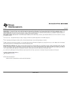
PACKAGE OPTION ADDENDUM

www.ti.com

9-Aug-2013

Addendum-Page 3

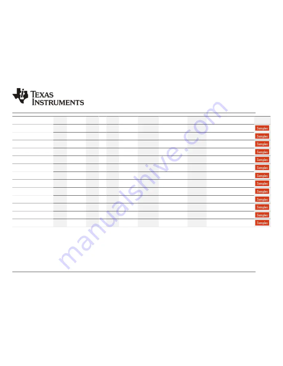
Orderable Device

Status

(1)

Package Type Package

Drawing

Pins Package

Qty

Eco Plan

(2)

Lead/Ball Finish

MSL Peak Temp

(3)

Op Temp (°C)

Device Marking

(4/5)

Samples

TLV4112IPE4

ACTIVE

PDIP

P

8

50

Pb-Free

(RoHS)

CU NIPDAU

N / A for Pkg Type

-40 to 125

TLV4112I

TLV4113CDGQ

ACTIVE

MSOP-

PowerPAD

DGQ

10

TBD

Call TI

Call TI

0 to 70

AHR

TLV4113CDGQG4

ACTIVE

MSOP-

PowerPAD

DGQ

10

TBD

Call TI

Call TI

0 to 70

AHR

TLV4113CDGQR

ACTIVE

MSOP-

PowerPAD

DGQ

10

2500

Green (RoHS

& no Sb/Br)

CU NIPDAU

Level-1-260C-UNLIM

0 to 70

AHR

TLV4113CDGQRG4

ACTIVE

MSOP-

PowerPAD

DGQ

10

2500

Green (RoHS

& no Sb/Br)

CU NIPDAU

Level-1-260C-UNLIM

0 to 70

AHR

TLV4113ID

ACTIVE

SOIC

D

14

50

Green (RoHS

& no Sb/Br)

CU NIPDAU

Level-1-260C-UNLIM

-40 to 125

4113I

TLV4113IDG4

ACTIVE

SOIC

D

14

50

Green (RoHS

& no Sb/Br)

CU NIPDAU

Level-1-260C-UNLIM

-40 to 125

4113I

TLV4113IDGQ

ACTIVE

MSOP-

PowerPAD

DGQ

10

80

Green (RoHS

& no Sb/Br)

CU NIPDAU

Level-1-260C-UNLIM

-40 to 125

AHS

TLV4113IDGQG4

ACTIVE

MSOP-

PowerPAD

DGQ

10

80

Green (RoHS

& no Sb/Br)

CU NIPDAU

Level-1-260C-UNLIM

-40 to 125

AHS

TLV4113IDGQR

ACTIVE

MSOP-

PowerPAD

DGQ

10

2500

Green (RoHS

& no Sb/Br)

CU NIPDAU

Level-1-260C-UNLIM

-40 to 125

AHS

TLV4113IDGQRG4

ACTIVE

MSOP-

PowerPAD

DGQ

10

2500

Green (RoHS

& no Sb/Br)

CU NIPDAU

Level-1-260C-UNLIM

-40 to 125

AHS

TLV4113IN

ACTIVE

PDIP

N

14

25

Pb-Free

(RoHS)

CU NIPDAU

N / A for Pkg Type

-40 to 125

TLV4113I

TLV4113INE4

ACTIVE

PDIP

N

14

25

Pb-Free

(RoHS)

CU NIPDAU

N / A for Pkg Type

-40 to 125

TLV4113I


(1)

 The marketing status values are defined as follows:

ACTIVE: Product device recommended for new designs.
LIFEBUY: TI has announced that the device will be discontinued, and a lifetime-buy period is in effect.
NRND: Not recommended for new designs. Device is in production to support existing customers, but TI does not recommend using this part in a new design.
PREVIEW: Device has been announced but is not in production. Samples may or may not be available.
OBSOLETE: TI has discontinued the production of the device.


(2)

 Eco Plan - The planned eco-friendly classification: Pb-Free (RoHS), Pb-Free (RoHS Exempt), or Green (RoHS & no Sb/Br) - please check 

http://www.ti.com/productcontent

 for the latest availability

information and additional product content details.
TBD:  The Pb-Free/Green conversion plan has not been defined.

Summary of Contents for TLV4110

Page 1: ... OF CHANNELS MSOP PDIP SOIC SHUTDOWN UNIVERSAL EVM BOARD TLV4110 1 8 8 8 Yes Refer to the EVM TLV4111 1 8 8 8 Refer to the EVM Selection Guide TLV4112 2 8 8 8 Selection Guide Lit SLOU060 TLV4113 2 10 14 14 Yes Lit SLOU060 HIGH LEVEL OUTPUT VOLTAGE vs HIGH LEVEL OUTPUT CURRENT VDD 3 V IOH High Level Output Current mA V OH High Level Output Voltage V TA 70 C TA 25 C TA 0 C TA 40 C 3 0 2 9 2 8 2 7 2 ...

Page 2: ... OUTLINE SYMBOL PLASTIC DIP P D SMALL OUTLINE DGN SYMBOL SMALL OUTLINE DGQ SYMBOL P 0 C to 70 C TLV4112CD TLV4112DGN xxTIAHP TLV4112CP 0 C to 70 C TLV4113CD TLV4113CDGQ xxTIAHR TLV4113CN 40 C to 125 C TLV4112ID TLV4112IDGN xxTIAHQ TLV4112IP 40 C to 125 C TLV4113ID TLV4113IDGQ xxTIAHS TLV4113IN This package is available taped and reeled To order this packaging option add an R suffix to the part num...

Page 3: ...to absolute maximum rated conditions for extended periods may affect device reliability NOTES 1 All voltage values except differential voltages are with respect to GND 2 To prevent permanent damage the die temperature must not exceed the maximum junction temperature DISSIPATION RATING TABLE PACKAGE θJC C W θJA C W TA 25 C POWER RATING TA 125 C POWER RATING D 8 38 3 176 710 mW 142 mW D 14 26 9 122 ...

Page 4: ...oltage VO PP 0 to 1V RL 10 kΩ Full range 75 dB AVD Large signal differential voltage amplification RL 100 Ω 25 C 88 94 dB amplification VDD 5 V RL 100 Ω Full range 75 VDD 5 V VO PP 0 to 3V RL 10 kΩ 25 C 90 110 VO PP 0 to 3V RL 10 kΩ Full range 85 Full range is 0 C to 70 C for C suffix and 40 C to 125 C for I suffix If not specified full range is 40 C to 125 C input characteristics PARAMETER TEST C...

Page 5: ... 38 0 6 V VDD 5 V VIC VDD 2 IOL 200 mA 40 C to 85 C 0 7 IO Output current Measured at 0 5 V from rail VDD 3 V 25 C 220 mA IO Output current Measured at 0 5 V from rail VDD 5 V 25 C 320 mA IOS Short circuit output current Sourcing 25 C 800 mA IOS Short circuit output current Sinking 25 C 800 mA Full range is 0 C to 70 C for C suffix and 40 C to 125 C for I suffix If not specified full range is 40 C...

Page 6: ...tortion performance PARAMETER TEST CONDITIONS TA MIN TYP MAX UNITS VO pp VDD 2 V AV 1 0 025 THD N Total harmonic distortion plus noise VO pp VDD 2 V RL 100 Ω f 100 Hz AV 10 0 035 THD N Total harmonic distortion plus noise RL 100 Ω f 100 Hz AV 100 25 C 0 15 Vn Equivalent input noise voltage f 100 Hz 25 C 55 nV Hz Vn Equivalent input noise voltage f 10 kHz 10 nV Hz In Equivalent input noise current ...

Page 7: ...ower supply voltage rejection ratio vs Frequency 10 AVD Differential voltage amplification and phase vs Frequency 11 Gain bandwidth product vs Supply voltage 12 SR Slew rate vs Supply voltage 13 SR Slew rate vs Temperature 14 Total harmonic distortion noise vs Frequency 15 Vn Equivalent input voltage noise vs Frequency 16 Phase margin vs Capacitive load 17 Voltage follower signal pulse response 18...

Page 8: ...2 0 0 50 200 100 150 250 300 2 2 2 1 TA 125 C Figure 5 TA 40 C LOW LEVEL OUTPUT VOLTAGE vs LOW LEVEL OUTPUT CURRENT VDD 3 V IOL Low Level Output Current mA TA 70 C TA 25 C TA 0 C OL V Low Level Output Voltage V 1 0 0 9 0 8 0 7 0 6 0 5 0 4 0 3 0 0 0 50 200 100 150 250 300 0 2 0 1 TA 125 C Figure 6 HIGH LEVEL OUTPUT VOLTAGE vs HIGH LEVEL OUTPUT CURRENT VDD 5 V IOH High Level Output Current mA V OH H...

Page 9: ... 5 2 0 1 5 1 0 0 5 0 0 Figure 13 0 00 0 25 0 50 0 75 1 00 1 25 1 50 1 75 2 00 SLEW RATE vs SUPPLY VOLTAGE AV 1 RL 100 Ω CL 10 pF VDD Supply Voltage V SR Slew Rate V µ s SR SR 2 5 3 4 5 3 5 4 5 5 5 6 Figure 14 0 00 0 25 0 50 0 75 1 00 1 25 1 50 1 75 2 00 40 25 10 5 20 35 50 65 80 95 110 125 SLEW RATE vs TEMPERATURE VDD 3 5 V AV 1 RL 100 Ω CL 10 pF TA Temperature C SR Slew Rate V µ s SR SR Figure 15...

Page 10: ...RTING LARGE SIGNAL PULSE RESPONSE t TIME µs 0 1 2 3 1 0 2 3 Output Voltage V V O V I Input Voltage V VDD 5 V AV 1 RL 100 Ω CL 50 pF TA 25 C VIN 2 5 V VIN VO 1 2 4 5 Figure 22 SMALL SIGNAL INVERTING PULSE RESPONSE t TIME µs 2 42 2 46 2 5 2 42 2 46 2 5 2 54 2 58 Output Voltage V V O V I Input Voltage V VDD 5 V AV 1 RL 100 Ω CL 50 pF TA 25 C VIN 2 5 V VIN VO 2 54 0 0 2 0 6 1 0 1 4 1 8 2 2 2 6 3 0 Fig...

Page 11: ...S 75265 TYPICAL CHARACTERISTICS 0 20 40 60 80 100 SHUTDOWN SUPPLY CURRENT OUTPUT VOLTAGE 120 Shutdown Supply Current I DD SD SHDN Shutdown Pulse V t Time µs 4 2 0 6 4 1 2 3 Output Voltage V V O 2 0 5 1 1 5 0 VDD 3 V AV 1 RL 100 Ω CL 10 pF VIN VDD 2 TA 25 C VO SD IDD SD µ A 0 Figure 26 ...

Page 12: ...e the operational amplifier into shutdown driving a capacitive load When the amplifier is configured in this manner capacitive loading directly on the output will decrease the device s phase margin leading to high frequency ringing or oscillations Therefore for capacitive loads of greater than 1 nF it is recommended that a resistor be placed in series RNULL with the output of the amplifier as show...

Page 13: ... or more of these factors results in a reduced die temperature The 8 pin SOIC small outline integrated circuit has a thermal impedance from junction to ambient of 176 C W For this reason it is recommended that the maximum power dissipation of the 8 pin SOIC package be limited to 350 mW with peak dissipation of 700 mW as long as the RMS value is less than 350 mW The use of the MSOP PowerPAD dramati...

Page 14: ...agement in one manufacturing operation During the surface mount solder operation when the leads are being soldered the thermal pad must be soldered to a copper area underneath the package Through the use of thermal paths within this copper area heat can be conducted away from the package into either a ground plane or other heat dissipating device Soldering the PowerPAD to the PCB is always recomme...

Page 15: ...l web or spoke via connection methodology Web connections have a high thermal resistance connection that is useful for slowing the heat transfer during soldering operations This makes the soldering of vias that have plane connections easier In this application however low thermal resistance is desired for the most efficient heat transfer Therefore the holes under the TLV411x PowerPAD package shoul...

Page 16: ...signer should never forget about the quiescent heat generated within the device especially multi amplifier devices Because these devices have linear output stages Class A B most of the heat dissipation is at low output voltages with high output currents The other key factor when dealing with power dissipation is how the devices are mounted on the PCB The PowerPAD devices are extremely useful for h...

Page 17: ...tional amplifier macromodel subcircuit updated using Model Editor release 9 1 on 01 18 00 at 15 50 Model Editor is an OrCAD product connections non inverting input inverting input positive power supply negative power supply output subckt TLV4112_5V 1 2 3 4 5 c1 11 12 2 2439E 12 c2 6 7 10 000E 12 css 10 99 454 55E 15 dc 5 53 dy de 54 5 dy dlp 90 91 dx dln 92 90 dx dp 4 3 dx egnd 99 0 poly 2 3 0 4 0...

Page 18: ...IP P 8 50 Pb Free RoHS CU NIPDAU N A for Pkg Type 40 to 125 TLV4110I TLV4110IPE4 ACTIVE PDIP P 8 50 Pb Free RoHS CU NIPDAU N A for Pkg Type 40 to 125 TLV4110I TLV4111CD ACTIVE SOIC D 8 75 Green RoHS no Sb Br CU NIPDAU Level 1 260C UNLIM 0 to 70 4111C TLV4111CDG4 ACTIVE SOIC D 8 75 Green RoHS no Sb Br CU NIPDAU Level 1 260C UNLIM 0 to 70 4111C TLV4111CDGN ACTIVE MSOP PowerPAD DGN 8 80 Green RoHS no...

Page 19: ...C UNLIM 0 to 70 AHP TLV4112CP ACTIVE PDIP P 8 50 Pb Free RoHS CU NIPDAU N A for Pkg Type 0 to 70 TLV4112C TLV4112CPE4 ACTIVE PDIP P 8 50 Pb Free RoHS CU NIPDAU N A for Pkg Type 0 to 70 TLV4112C TLV4112ID ACTIVE SOIC D 8 75 Green RoHS no Sb Br CU NIPDAU Level 1 260C UNLIM 40 to 125 4112I TLV4112IDG4 ACTIVE SOIC D 8 75 Green RoHS no Sb Br CU NIPDAU Level 1 260C UNLIM 40 to 125 4112I TLV4112IDGN ACTI...

Page 20: ...NIPDAU Level 1 260C UNLIM 40 to 125 AHS TLV4113IDGQR ACTIVE MSOP PowerPAD DGQ 10 2500 Green RoHS no Sb Br CU NIPDAU Level 1 260C UNLIM 40 to 125 AHS TLV4113IDGQRG4 ACTIVE MSOP PowerPAD DGQ 10 2500 Green RoHS no Sb Br CU NIPDAU Level 1 260C UNLIM 40 to 125 AHS TLV4113IN ACTIVE PDIP N 14 25 Pb Free RoHS CU NIPDAU N A for Pkg Type 40 to 125 TLV4113I TLV4113INE4 ACTIVE PDIP N 14 25 Pb Free RoHS CU NIP...

Page 21: ...5 Multiple Device Markings will be inside parentheses Only one Device Marking contained in parentheses and separated by a will appear on a device If a line is indented then it is a continuation of the previous line and the two combined represent the entire Device Marking for that device Important Information and Disclaimer The information provided on this page represents TI s knowledge and belief ...

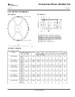
Page 22: ...DGN 8 2500 330 0 12 4 5 3 3 4 1 4 8 0 12 0 Q1 TLV4111IDR SOIC D 8 2500 330 0 12 4 6 4 5 2 2 1 8 0 12 0 Q1 TLV4112IDGNR MSOP Power PAD DGN 8 2500 330 0 12 4 5 3 3 4 1 4 8 0 12 0 Q1 TLV4112IDGNR MSOP Power PAD DGN 8 2500 330 0 12 4 5 3 3 4 1 4 8 0 12 0 Q1 TLV4112IDR SOIC D 8 2500 330 0 12 4 6 4 5 2 2 1 8 0 12 0 Q1 TLV4113CDGQR MSOP Power PAD DGQ 10 2500 330 0 12 4 5 3 3 4 1 4 8 0 12 0 Q1 TLV4113IDGQ...

Page 23: ... PowerPAD DGN 8 2500 358 0 335 0 35 0 TLV4111IDR SOIC D 8 2500 340 5 338 1 20 6 TLV4112IDGNR MSOP PowerPAD DGN 8 2500 358 0 335 0 35 0 TLV4112IDGNR MSOP PowerPAD DGN 8 2500 364 0 364 0 27 0 TLV4112IDR SOIC D 8 2500 340 5 338 1 20 6 TLV4113CDGQR MSOP PowerPAD DGQ 10 2500 358 0 335 0 35 0 TLV4113IDGQR MSOP PowerPAD DGQ 10 2500 358 0 335 0 35 0 PACKAGE MATERIALS INFORMATION www ti com 12 Dec 2011 Pac...

Page 24: ......

Page 25: ......

Page 26: ......

Page 27: ......

Page 28: ......

Page 29: ......

Page 30: ......

Page 31: ......

Page 32: ......

Page 33: ......

Page 34: ......

Page 35: ...esponsible for compliance with all legal regulatory and safety related requirements concerning its products and any use of TI components in its applications notwithstanding any applications related information or support that may be provided by TI Buyer represents and agrees that it has all the necessary expertise to create and implement safeguards which anticipate dangerous consequences of failur...

Reviews: