www.ti.com
2
SRIO Functional Description
2.1
Overview
2.1.1
Peripheral Data Flow
SRIO Functional Description
This peripheral is designed to be an externally driven slave module that is capable of acting as a master in
the DSP system. This means that an external device can push (burst write) data to the DSP as needed,
without having to generate an interrupt to the CPU or without relying on the DSP EDMA. This has several
benefits. It cuts down on the total number of interrupts, it reduces handshaking (latency) associated with
read-only peripherals, and it frees up the EDMA for other tasks.
SRIO specifies data packets with payloads up to 256 bytes. Many times, transactions will span across
multiple packets. RapidIO specifies a maximum of 16 transactions per message. Although a request is
generated for each packet transaction so that the DMA can transfer the data to L2 memory, an interrupt is
only generated after the final packet of the message. This interrupt notifies the CPU that data is available
in L2 Memory for processing.
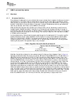
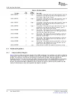
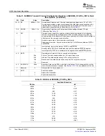
As an endpoint device, the peripheral accepts packets based on the destination ID. Two options exist for
packet acceptance and are mode selectable. The first option is to only accept packets whose DestIDs
match the local deviceID in 0x0080. This provides a level of security. The second option is is system
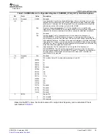
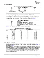
multicast operation. When multicast is enabled in SP_IP_MODE (offset 12004h) bit 5, incoming packets
matching the deviceID in the registers shown in are accepted.
Table 2. Registers Checked for Multicast DeviceID
Registers Checked For Multicast DeviceID
Device
Name
Address Offset
TMS320TCI6482
Local DeviceID Register
0080h
Multicast DeviceID Register
0084h
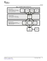
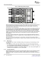
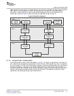
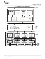
Data flow through the peripheral can be explained using the high-level block diagram shown in
Figure 4
.
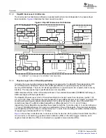
High-speed data enters from the device pins into the RX block of the SERDES macro. The RX block is a
differential receiver expecting a minimum of 175mV peak-to-peak differential input voltage (Vid). Level
shifting is performed in the RX block, such that the output is single ended CMOS. The serial data is then
fed to the SERDES clock recovery block. The sole purpose of this block is to extract a clock signal from
the data stream. To do this, a low-frequency reference clock is required. Typically, this clock comes from
an off-chip stable crystal oscillator and is a LVDS device input separate to the SERDES. This clock is
distributed to the SERDES PLL block which multiplies that frequency up to that of the data rate. Multiple
high-speed clock phases are created and routed to the clock recovery blocks. The clock recovery blocks
further interpolate between these clocks to provide maximum Unit Interval (UI) resolution on the recovered
clock. The clock recovery block samples the incoming data and monitors the relative positions of the data
edges. With this information, it can provide the data and a center-aligned clock to the S2P block. The S2P
block uses the newly recovered clock to de-multiplex the data into 10-bit words. At this point, the data
leaves the SERDES macro at 1/10th the pin data rate, accompanied by an aligned byte clock.
SPRUE13A – September 2006
Serial RapidIO (SRIO)
21
Submit Documentation Feedback

