background image

SRIO Registers

BYTE_COUNT field of LSUn_REG3

158

B

bad CRC in control symbol at port n

C

rate counting enable field

221

CAPTURE0 field of SPn_ERR_CAPT_DBG1

224

status field

219

CAPTURE1 field of SPn_ERR_CAPT_DBG2

225

bad CRC in packet at port n

CAPTURE2 field of SPn_ERR_CAPT_DBG3

226

rate counting enable field

222

CAPTURE3 field of SPn_ERR_CAPT_DBG4

227

status field

220

CAPTURE_VALID_INFO field of

bandwidth per differential pair based on 1x/4x LP-Serial

SPn_ERR_ATTR_CAPT_DBG0

223

specification

18

CBA_TRANS_PRI field of PER_SET_CNTL

113

BASE_DEVICEID field of BASE_ID

193

cc field of RX buffer descriptor

47

BASE_ID

193

cc field of TX buffer descriptor

52

base address registers for local configuration space

CDR field of SERDES_CFGRXn_CNTL

125

191, 192

CLASS field of PID

111

base device ID CSR

193

clearing interrupt conditions

86

base device ID for host PE

194

clear registers

Big Endian versus Little Endian

68

for CPPI interrupt conditions

135, 137

binary notational convention

14

for doorbell interrupt conditions

133

BLK0_EN_STAT field of GBL_EN_STAT

117

for error, reset, and special event (port) interrupt

BLK1_EN_STAT field of GBL_EN_STAT

117

conditions

143

BLK2_EN_STAT field of GBL_EN_STAT

117

for LSU interrupt conditions

141

BLK3_EN_STAT field of GBL_EN_STAT

117

clock/data recovery field

125

BLK4_EN_STAT field of GBL_EN_STAT

117

clock domains

21

BLK5_EN_STAT field of GBL_EN_STAT

117

clock prescaler field

233

BLK6_EN_STAT field of GBL_EN_STAT

117

clock recovery

21

BLK7_EN_STAT field of GBL_EN_STAT

117

CMD field of SPn_CS_TX

240

BLK8_EN_STAT field of GBL_EN_STAT

117

CM field of SERDES_CFGTXn_CNTL

128

BLKn_EN

119

CNTL_SYM_UNEXPECTED_ACKID_EN field of

BLKn_EN_STAT

120

SPn_RATE_EN

221

block 0 enable status bit

118

CNTL_SYM_UNEXPECTED_ACKID field of

block 1 enable status bit

117

SPn_ERR_DET

219

block 2 enable status bit

117

command control symbol field for port n

240

block 3 enable status bit

117

COMMAND field of SPn_LM_REQ

200

block 4 enable status bit

117

command status (completion code) field for LSUn

161

block 5 enable status bit

117

common mode field

128

block 6 enable status bit

117

common transport large system support field

186

block 7 enable status bit

117

Communications Port Programming Interface. See CPPI

block 8 enable status bit

117

43

block diagram of SRIO components

26

COMP_TAG

195

block diagram of SRIO peripheral

21

COMPLETION_CODE field of LSUn_REG6

161

block enable registers

119

completion pointer for RX queue n

167

block enable status registers

120

completion pointer for TX queue n

165

BOOT_COMPLETE field of PER_SET_CNTL

113

COMPONENT_TAG field of COMP_TAG

195

bootloading

configuration offset field for LSUn

156

access to read-only registers

113

configuring SERDES macros

28

configuration and operation

79

congestion control

65

data movement

80

basic scheme

66

device wakeup afterwards

80

congestion control packet (CCP) Ftype and Ttype

25

BRIDGE field of PE_FEAT

186

congestion control packet (CCP) purpose

65

bridge present field

186

count of Xoff congestion control packets

66

BSY field of LSUn_REG6

161

flow control destination IDs

66

buffer_pointer field of RX buffer descriptor

47

flow masks

67

buffer_pointer field of TX buffer descriptor

52

time-out timer

66

BUSWIDTH field of SERDES_CFGRXn_CNTL

125

control capture CSR for logical/transport errors

217

BUSWIDTH field of SERDES_CFGTXn_CNTL

128

control information field for port n error capture

224

busy (BSY) signal of an LSU

39

control symbols

busy status field for LSUn

161

acknowledge or link-response control symbol overdue

242

Index

SPRUE13A – September 2006

Submit Documentation Feedback

Summary of Contents for TMS320TCI648x

Page 1: ...TMS320TCI648x Serial RapidIO SRIO User s Guide Literature Number SPRUE13A September 2006...

Page 2: ...2 SPRUE13A September 2006 Submit Documentation Feedback...

Page 3: ...Global Enable Status Register GBL_EN_STAT 117 5 7 Block n Enable Register BLKn_EN 119 5 8 Block n Enable Status Register BLKn_EN_STAT 120 5 9 RapidIO DEVICEID1 Register DEVICEID_REG1 121 5 10 RapidIO...

Page 4: ...ter QUEUEn_TXDMA_CP 165 5 43 Queue n Receive DMA Head Descriptor Pointer Register QUEUEn_RXDMA_HDP 166 5 44 Queue n Receive DMA Completion Pointer Register QUEUEn_RXDMA_CP 167 5 45 Transmit Queue Tear...

Page 5: ...able CSR n SPn_RATE_EN 221 5 84 Port n Attributes Error Capture CSR 0 SPn_ERR_ATTR_CAPT_DBG0 223 5 85 Port n Error Capture CSR 1 SPn_ERR_CAPT_DBG1 224 5 86 Port n Error Capture CSR 2 SPn_ERR_CAPT_DBG2...

Page 6: ...7E0h 7ECh 56 24 RX Buffer Descriptors 62 25 TX Buffer Descriptors 63 26 Doorbell Operation 64 27 Flow Control Table Entry Registers Address Offset 0900h 093Ch 66 28 Transmit Source Flow Control Masks...

Page 7: ...r n SERDES_CFGTXn_CNTL 128 76 SERDES Macro Configuration Register n SERDES_CFGn_CNTL 130 77 Doorbell n Interrupt Condition Status Register DOORBELLn_ICSR 132 78 Doorbell n Interrupt Condition Clear Re...

Page 8: ...TAG Address Offset 106Ch 195 128 1x 4x LP_Serial Port Maintenance Block Header Register SP_MB_HEAD Address Offset 1100h 196 129 Port Link Time Out Control CSR SP_LT_CTL Address Offset 1120h 197 130 Po...

Page 9: ...Port Reset Option CSR n SPn_RST_OPT 235 159 Port Control Independent Register n SPn_CTL_INDEP 236 160 Port Silence Timer n Register SPn_SILENCE_TIMER 238 161 Port Multicast Event Control Symbol Reque...

Page 10: ...70 27 Global Enable and Global Enable Status Field Descriptions 72 28 Block Enable and Block Enable Status Field Descriptions 73 29 Peripheral Control Register PCR Field Descriptions 74 30 Port Mode...

Page 11: ...8 74 LSU Interrupt Condition Clear Register LSU_ICCR Field Descriptions 141 75 Error Reset and Special Event Interrupt Condition Status Register ERR_RST_EVNT_ICSR Field Descriptions 142 76 Error Reset...

Page 12: ...ions 182 124 Device Information CAR DEV_INFO Field Descriptions 183 125 Assembly Identity CAR ASBLY_ID Field Descriptions 184 126 Assembly Information CAR ASBLY_INFO Field Descriptions 185 127 Process...

Page 13: ...Registers and the Associated Ports 226 169 Port n Error Capture CSR 3 SPn_ERR_CAPT_DBG3 Field Descriptions 226 170 SPn_ERR_CAPT_DBG4 Registers and the Associated Ports 227 171 Port n Error Capture CSR...

Page 14: ...his solution are met therefore no electrical data timing information is supplied here for this interface TMS320C6000 CPU and Instruction Set Reference Guide literature number SPRU189 gives an introduc...

Page 15: ...MS320C62x TMS320C67x TMS320C6000 Code Composer Studio are trademarks of Texas Instruments RapidIO is a registered trademark of RapidIO Trade Association InfiniBand is a trademark of the InfiniBand Tra...

Page 16: ...ory subsystems and general purpose computing Principle features of RapidIO include Flexible system architecture allowing peer to peer communication Robust communication with error detection features F...

Page 17: ...ress Information to transport packet from end Transport specification spec transport Common between two physical devices i e electrical Information necessary to move packet interface flow control Phys...

Page 18: ...clock recovery interface The two physical layer specifications are not compatible SRIO complies with the 1x 4x LP Serial specification The serializer deserializer SERDES technology in SRIO also align...

Page 19: ...ifferential CML signaling supporting AC coupling Support for 1 25 2 5 and 3 125 Gbps rates Power down option for unused ports Read write write with response streaming write outgoing Atomic and mainten...

Page 20: ...l Specification These and the various associated documents listed herein can be found at the official RapidIO website www RapidIO org SRIO provides a seamless interface to all devices which are compli...

Page 21: ...gisters Checked for Multicast DeviceID Registers Checked For Multicast DeviceID Device Name Address Offset TMS320TCI6482 Local DeviceID Register 0080h Multicast DeviceID Register 0084h Data flow throu...

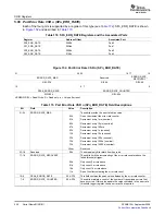
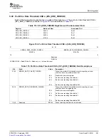
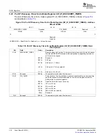
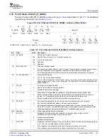
Page 22: ...he FIFO the four lanes are synchronized in frequency and phase whether 1X or 4X mode is being used The FIFO is 8 words deep The lane de skew is only meaningful in the 4X mode where it aligns each chan...

Page 23: ...enance functions Figure 5 shows how a packet progresses through the system Figure 5 Operation Sequence An example packet is shown as two data streams in Figure 6 The first is for payload sizes of 80 b...

Page 24: ...cket Accepted control symbol is sent by the receiving device If the CRC is incorrect a Packet Not Accepted control symbol is sent so that transmission may be retried Control symbols are physical layer...

Page 25: ...E Ttype 0101b NWRITE_R Ttype 1110b Atomic test and swap Ttype others Ftype 6 Ttype don t care SWRITE Ftype 7 Ttype don t care Congestion control Ftype 8 Ttype 0000b Maintenance read Ttype 0001b Mainte...

Page 26: ...e Data Differential point to point unidirectional bus Receives packet data for a transmitting device s TX pins Bit used in 4 port 1x device and 1 port 4X device RIORX1 RIORX1 2 Input Receive Data Diff...

Page 27: ...276B 8 buffers per 1X port all priorities 32 buffers per 4X port 8 per priority Transaction mapping layer buffers Logical Load Store units LSUs TX direct I O Maintenance Messaging TXU RX direct I O MA...

Page 28: ...serial to parallel S2P and parallel to serial P2S blocks The internal PLL multiplies a user supplied reference clock All loop filter components of the PLL are onchip Likewise the differential TX and R...

Page 29: ...ing may offer better performance It will reduce the amount of reference clock jitter transferred through the PLL However it also increases the susceptibility to loop noise generated within the PLL its...

Page 30: ...Line Rate Range Gbps MPY Range MHz Full Half Quarter 4x 250 425 2 3 4 1 1 7 0 5 0 85 5x 200 425 2 4 25 1 2 125 0 5 1 0625 6x 167 354 167 2 4 25 1 2 125 0 5 1 0625 8x 125 265 625 2 4 25 1 2 125 0 5 1 0...

Page 31: ...gic analyzes data patterns and transition times to determine whether the low frequency gain of the equalizer should be increased or decreased For the fully adaptive setting EQ 0001 if the low frequenc...

Page 32: ...on with 2 selectable thresholds 00b Disabled Loss of signal detection disabled 01b High threshold Loss of signal detection threshold in the range 85 to 195mVdfpp This setting is suitable for Infiniban...

Page 33: ...transmitter will be disabled and clocks will be gated off with the exception of the transmit clock TXBCLK n output which will continue to operate normally All current sources within the transmitter wi...

Page 34: ...NVPAIR Invert polarity Inverts the polarity of RIOTXn and RIOTXn 0 Normal polarity RIOTXn is considered to be positive data and RIOTXn negative 1 Inverted polarity RIOTXn is considered to be negative...

Page 35: ...ice Direct I O requires that a RapidIO source device keep a local table of addresses for memory within the destination device Once these tables are established the RapidIO source controller uses this...

Page 36: ...5 and 6 Will be used in conjunction with BYTE_COUNT to LSB Config_offset create 64 bit aligned RapidIO packet header address 2 24 bit Config_offset Field Maintenance Packets Type 8 Will be used in con...

Page 37: ...se payload length was in error 100b Transaction complete packet not sent due to unsupported transaction type or invalid programming encoding for one or more LSU register fields 101b DMA data transfer...

Page 38: ...LSU1_REG2 CSL_FMK SRIO_LSU1_REG2_DSP_ADDRESS int xmtBuff1 0 SRIO_REGS LSU1_REG3 CSL_FMK SRIO_LSU1_REG3_BYTE_COUNT byte_count SRIO_REGS LSU1_REG4 CSL_FMK SRIO_LSU1_REG4_OUTPORTID 0 CSL_FMK SRIO_LSU1_R...

Page 39: ...packets are generated through this interface The data path for this module uses DMA bus as the DMA interface The configuration bus is used by the CPU to access the control command registers The regist...

Page 40: ...ne payload can be completed in any single DMA bus cycle The Load Store module can only forward the packet to the TX FIFO after the final payload byte from the DMA bus response has been written into th...

Page 41: ...rs are written using the configuration bus Flow control is determined TX FIFO free buffer availability is determined DMA bus read request for data payload DMA bus response writes data to specified mod...

Page 42: ...x LP Serial Specification If the time expires control command register resources should be released and an error is logged in the error management RapidIO registers The RapidIO Interconnect Specificat...

Page 43: ...iding 256 messages Mailboxes can be defined for different data types or priorities The advantage of message passing is that the source device does not require any knowledge of the destination device s...

Page 44: ...given segment of a message DestID is equal to port for TX operations and the same DestID is not accessible from multiple ports As message packets are received by the RapidIO ports the data is written...

Page 45: ...all zeros would allow a mapping entry to be used for all incoming mailboxes The mapping table entry also provides a security feature to enable or disable access from specific external devices to loca...

Page 46: ...the RX DMA State Registers Table 16 RX DMA State Head Descriptor Pointer HDP Address Offset 600h 63Ch Bit Name Description 31 0 RX Queue Head RX Queue Head Descriptor Pointer This field is the memory...

Page 47: ...e queue As segments of a received message arrive the msgseg field of each segment is monitored to detect the completion of the received message Once a full message is received the OWNERSHIP bit is cle...

Page 48: ...y the peripheral after receiving a message to indicate the actual number of double words in the entire message Message payloads are limited to a maximum size of 512 double words 4096 bytes 000000000b...

Page 49: ...rces subsequent pipelined messages may arrive just as resources are freed up This is a problem for systems requiring in order message delivery In this case the peripheral needs to record the Src_id ma...

Page 50: ...ueue will be torn down and reported with the current buffer descriptor teardown bit set ownership bit cleared CC 100b All other fields of the buffer descriptor are invalid The peripheral completes the...

Page 51: ...the queue transmit For TX operation PortID is specified to direct the outgoing packet to the appropriate port Table 19 and Table 20 describe the TX DMA state registers Figure 22 shows the TX buffer d...

Page 52: ...r The byte aligned memory address of the buffer associated with the buffer descriptor The DSP core sets the buffer_pointer sop 1 Start of Message Indicates that the descriptor buffer is the first buff...

Page 53: ...code indicates an error in one or more segments of a transmitted multi segment message message_length Message Length Message Length Written by the DSP core to specify the number of double words to tra...

Page 54: ...that queue are stalled To counter the effects and reduce back up of more TX packets multiple queues are available The peripheral supports a total of 16 assignable TX queues and their associated TX DMA...

Page 55: ...eral can re order packets of different priorities when fabric congestion occurs If message ordering is needed the following must be obeyed Multi Segmented Messages If there are only two devices A send...

Page 56: ...eue Pointer Number of Msgs Queue Pointer R W 0h R W 9h R W 0h R W 8h TX_QUEUE_CNTL3 Address Offset 7ECh TX_Queue_Map15 TX_Queue_Map14 31 28 27 24 23 20 19 16 Number of Msgs Queue Pointer Number of Msg...

Page 57: ...TX_Queue_Map6 TX_QUEUE_CNTL1 19 16 Queue Pointer 0h to Fh Pointer to a queue This pointer can be programmed to point to any one of the 16 TX buffer descriptor queues TX_QUEUE_CNTL1 23 20 Number of Msg...

Page 58: ...sage buffer descriptors The software manages the queue usage All outgoing message segments have responses that indicate the status of the transaction Responses may indicate DONE ERROR or RETRY A buffe...

Page 59: ...times out Note that normal TX State Machine operation is to not send any more segments once an error response has been received on any segment So if the receiver has also been torn down and is receivi...

Page 60: ...ue in the RX DMA State CP register Resets interrupt pacing value TX Operation Sets up associated buffer descriptor memory CPPI RAM or L2 RAM Link lists the buffer descriptors next_descriptor_pointer A...

Page 61: ...ffer Descriptor RX_DESCP0_0 RXDESC0 CSL_FMK SRIO_RXDESC0_N_POINTER int RX_DESCP0_1 link to RX_DESCP0_1 RX_DESCP0_0 RXDESC1 CSL_FMK SRIO_RXDESC1_B_POINTER int rcvBuff1 0 RX_DESCP0_0 RXDESC2 CSL_FMK SRI...

Page 62: ...K SRIO_TXDESC3_OWNERSHIP 1 CSL_FMK SRIO_TXDESC3_EOQ 1 CSL_FMK SRIO_TXDESC3_TEARDOWN 0 CSL_FMK SRIO_TXDESC3_RETRY_COUNT 0 CSL_FMK SRIO_TXDESC3_MESSAGE_LENGTH MLEN_512DW TX_DESCP0_1 TXDESC0 CSL_FMK SRIO...

Page 63: ...as error indicators or status information from a device that does not contain an endpoint such as a switch The data payload is typically placed in a queue in the targeted endpoint and an interrupt is...

Page 64: ...it can be assigned to any core as described below by the Interrupt Condition Routing Registers Additionally each status bit is user defined for the application For instance it may be desirable to supp...

Page 65: ...omic transactions are not allowed Atomic test and swap operations Ftype 5 to external devices are limited to a payload of one double word 8 bytes These operations are like NWRITE with response 55h tra...

Page 66: ...Instead of dynamically updating a table with each CCP s flow information as it arrives a small finite entry table is set up and configured by software to reflect the more critical flows it is using On...

Page 67: ...he 8 MSBs of this field are don t care bits Each transmit source including any LSU and any TX CPPI queue indicates which of the 16 flows it uses with a 16 bit flow mask Figure 28 illustrates the regis...

Page 68: ...ow 4 from table entry 3 FL3 0 TX source does not support Flow 3 from table entry 1 TX source supports Flow 3 from table entry 2 FL2 0 TX source does not support Flow 2 from table entry 1 TX source sup...

Page 69: ...ccesses are performed on 32 bit values at a fixed address position The bit positions in the 32 bit word are defined by this specification This means that a memory image which will be copied to a MMR i...

Page 70: ...to bit 0 of the SERDES_CFGTXn_CNTL and SERDES_CFGRXn_CNTL registers The PLL and remaining SERDES functional blocks can be controlled by writing to the ENPLL signal in the SERDES_CFG0_CNTL register Th...

Page 71: ...the peripheral and its partner are fully initialized and ready for normal operation the peripheral will not send any data packets or non status control symbols GBL_EN Resets all MMRs excluding Reset...

Page 72: ...0 Logical block 4 is in reset with its clock off 1 Logical block 4 is enabled with its clock running GBL_EN_STAT 4 BLK3_EN_STAT Block 3 enable status Logical block 3 is the message transmit unit TXU...

Page 73: ...AT Address 007Ch 31 1 0 Reserved EN_STAT R 0 R 1 LEGEND R Read W Write n Value after reset Table 28 Block Enable and Block Enable Status Field Descriptions Register Bit Field Valu Description e BLKn_E...

Page 74: ...channel is used for driving the LSU it must be stopped to prevent new additional transfers This procedure is outside the scope of this specification Teardown of the TXU queues is accomplished by writ...

Page 75: ...is available in the peripheral the peripheral services externally generated requests as long as possible When the internal buffers are consumed the peripheral will retry incoming network packets in t...

Page 76: ...riorities 0 0 1 2 3 3 1 0 where the leftmost 0 represents the packet that was the first in or head of the queue If this packet is retried the next packet to be sent is the earliest packet with priorit...

Page 77: ...SRIO_REGS BLK0_EN 0x00000001 MMR_EN SRIO_REGS BLK5_EN 0x00000001 PORT0_EN SRIO_REGS BLK1_EN 0x00000001 LSU_EN SRIO_REGS BLK2_EN 0x00000001 MAU_EN SRIO_REGS BLK3_EN 0x00000001 TXU_EN SRIO_REGS BLK4_EN...

Page 78: ...SRIO_REGS PER_SET_CNTL data 0x00000000 mask 0x01000000 mdata wdata mask rdata mask SRIO_REGS PER_SET_CNTL mdata bootcmpl 0 SRIO_REGS DEV_ID 0xBEEF0030 id BEEF ti 0x0030 SRIO_REGS DEV_INFO 0x00000000 0...

Page 79: ...0x00000002 0x00000002 rdata SRIO_REGS P0_ERR_STAT if srio4p1x_mode rdata SRIO_REGS P1_ERR_STAT while rdata 0x00000002 0x00000002 rdata SRIO_REGS P1_ERR_STAT rdata SRIO_REGS P2_ERR_STAT while rdata 0x0...

Page 80: ...n a manner similar to that described in Section 4 monitoring the DMA bus write with response commands to ensure that the data has been completely transferred through the DMA This interrupt wakes up th...

Page 81: ...rded based on the rules outlined in Section 2 3 15 1 If the packet s DestID doesn t match either the packet is simply destroyed or forwarded depending on the whether the hardware packet forwarding is...

Page 82: ...r n for 8 Bit DeviceIDs PF_8B_CNTLn Field Descriptions Bit Field Value Description 31 18 Reserved 0 Reserved 17 16 OUT_BOUND_PORT 0 3 Output port number for packets whose DestID falls within the 8 bit...

Page 83: ...ERROR response to an IO logical layer request To clear this bit write 0 to it 30 MSG_ERR_RSPNS Message error response endpoint device only 0 The TXU did not receive an ERROR response to a message log...

Page 84: ...icited response packet has not been received by an LSU or the TXU 1 An unsolicited response packet has been received by an LSU or the TXU To clear this bit write 0 to it 22 UNSUPPORTED_TRANS Unsupport...

Page 85: ...t I O protocol When the single or multi packet data transfer is complete the external PE or the peripheral itself must notify the local processor that the data is available for processing To avoid err...

Page 86: ...implemented at the peripheral level to manage the interrupt rate as described in Section 4 7 Error handling on the RapidIO link is handled by the peripheral and as such does not require the interventi...

Page 87: ...16 Reserved R 0 15 14 13 12 11 10 9 8 7 6 5 4 3 2 1 0 ICS15 ICS14 ICS13 ICS12 ICS11 ICS10 ICS9 ICS8 ICS7 ICS6 ICS5 ICS4 ICS3 ICS2 ICS1 ICS0 R 0 R 0 R 0 R 0 R 0 R 0 R 0 R 0 R 0 R 0 R 0 R 0 R 0 R 0 R 0...

Page 88: ...R 0 Doorbell 3 Interrupt Condition Clear Register DOORBELL3_ICCR Address Offset 0238h 31 16 Reserved R 0 15 14 13 12 11 10 9 8 7 6 5 4 3 2 1 0 ICC15 ICC14 ICC13 ICC12 ICC11 ICC10 ICC9 ICC8 ICC7 ICC6 I...

Page 89: ...0 W 0 W 0 W 0 LEGEND R Read only W Write only n Value after reset Figure 51 TX CPPI Interrupt Condition Status and Clear Registers TX CPPI Interrupt Condition Status Register TX_CPPI_ICSR Address Offs...

Page 90: ...LSU4 Transaction was not sent due to Xoff condition 25 LSU4 Non posted transaction received ERROR response or error in response payload 24 LSU4 Transaction complete No errors posted non posted 1 23 LS...

Page 91: ...ST_EVNT_ICCR are used to clear the corresponding ICS bits Figure 53 Error Reset and Special Event Interrupt Condition Status and Clear Registers Error Reset and Special Event Interrupt Condition Statu...

Page 92: ...1 to clear Write 1 to clear any of the Write 1 to clear following possible bits Offset 0x0278 Offset 0x2040 Offset 0x14004 ERR_RST_EVNT_ICCR 8 SP0_ERR_STAT 2 Fatal SP0_CTL_INDEP 6 error SP0_ERR_STAT 2...

Page 93: ...support four CPU servicing interrupt destinations one per core INTDST0 for Core0 INTDST1 for Core1 INTDST2 for Core2 and INTDST3 for Core3 In addition INTDST4 may be globally routed to all cores and...

Page 94: ...Value after reset Figure 55 shows the ICRRs for the RXU and Figure 56 shows the ICRRs for the TXU These registers route queue interrupts to interrupt destinations For example if ICS6 1 in RX_CPPI_ICS...

Page 95: ...TX_CPPI_ICRR2 Address Offset 02D4h 31 28 27 24 23 20 19 16 ICR15 ICR14 ICR13 ICR12 R W 0000 R W 0000 R W 0000 R W 0000 15 12 11 8 7 4 3 0 ICR11 ICR10 ICR9 ICR8 R W 0000 R W 0000 R W 0000 R W 0000 LEG...

Page 96: ...ition Routing Register 2 LSU_ICRR2 Address Offset 02E8h 31 28 27 24 23 20 19 16 ICR23 ICR22 ICR21 ICR20 R W 0000 R W 0000 R W 0000 R W 0000 15 12 11 8 7 4 3 0 ICR19 ICR18 ICR17 ICR16 R W 0000 R W 0000...

Page 97: ...230 Doorbell3 interrupts 0x0240 RX CPPI interrupts 0x0250 TX CPPI interrupts 0x0260 LSU interrupts 0x0270 Error Reset and Special Event interrupts To reduce the number of reads up to 5 reads required...

Page 98: ...E 31 30 29 28 27 26 25 24 23 22 21 20 19 18 17 16 ISD31 ISD30 ISD29 ISD28 ISD27 ISD26 ISD25 ISD24 ISD23 ISD22 ISD21 ISD20 ISD19 ISD18 ISD17 ISD16 R 0 R 0 R 0 R 0 R 0 R 0 R 0 R 0 R 0 R 0 R 0 R 0 R 0 R...

Page 99: ...n Regardless of the interrupt sources the physical interrupts are set only when the total number of set ICSR bits transitions from none to one or more The peripheral is responsible for setting the cor...

Page 100: ...tes all pending interrupts and re pulses the interrupt signal if any interrupt conditions are pending The down counter is based on the DMA clock cycle Figure 62 INTDSTn_RATE_CNTL Interrupt Rate Contro...

Page 101: ...emp2 SRIO_REGS RX_CPPI_ICSR if temp2 0x00000001 0x00000001 SRIO_REGS Queue0_RXDMA_CP int RX_DESCP0_0 SRIO_REGS DOORBELL0_ICCR 0xFFFFFFFF SRIO_REGS DOORBELL1_ICCR 0xFFFFFFFF SRIO_REGS DOORBELL2_ICCR 0x...

Page 102: ...le Status 7 Section 5 8 0078h BLK8_EN Block Enable 8 Section 5 7 007Ch BLK8_EN_STAT Block Enable Status 8 Section 5 8 0080h DEVICEID_REG1 RapidIO DEVICEID1 Register Section 5 9 0084h DEVICEID_REG2 Rap...

Page 103: ...ndition Clear Section 5 25 Register 0280h DOORBELL0_ICRR DOORBELL0 Interrupt Condition Routing Register Section 5 26 0284h DOORBELL0_ICRR2 DOORBELL 0 Interrupt Condition Routing Register 2 Section 5 2...

Page 104: ...h LSU1_REG6 LSU1 Control Register 6 Section 5 39 041Ch LSU1_FLOW_MASKS LSU1 Congestion Control Flow Mask Register Section 5 40 0420h LSU2_REG0 LSU2 Control Register 0 Section 5 33 0424h LSU2_REG1 LSU2...

Page 105: ...letion Pointer Register 6 Section 5 42 059Ch QUEUE7_TXDMA_CP Queue Transmit DMA Completion Pointer Register 7 Section 5 42 05A0h QUEUE8_TXDMA_CP Queue Transmit DMA Completion Pointer Register 8 Sectio...

Page 106: ...X_CPPI_FLOW_MASKS2 Transmit CPPI Supported Flow Mask Register 2 Section 5 46 0710h TX_CPPI_FLOW_MASKS3 Transmit CPPI Supported Flow Mask Register 3 Section 5 46 0714h TX_CPPI_FLOW_MASKS4 Transmit CPPI...

Page 107: ...ox to Queue Mapping Register H17 Section 5 50 0890h RXU_MAP_L18 MailBox to Queue Mapping Register L18 Section 5 50 0894h RXU_MAP_H18 MailBox to Queue Mapping Register H18 Section 5 50 0898h RXU_MAP_L1...

Page 108: ...tion 5 51 1000h DEV_ID Device Identity CAR Section 5 52 1004h DEV_INFO Device Information CAR Section 5 53 1008h ASBLY_ID Assembly Identity CAR Section 5 54 100Ch ASBLY_INFO Assembly Information CAR S...

Page 109: ...CSR 1 Section 5 85 2050h SP0_ERR_CAPT_DBG2 Port 0 Packet Control Symbol Error Capture CSR 2 Section 5 86 2054h SP0_ERR_CAPT_DBG3 Port 0 Packet Control Symbol Error Capture CSR 3 Section 5 87 2058h SP0...

Page 110: ...0 Reset Option CSR Section 5 95 14004h SP0_CTL_INDEP Port 0 Control Independent Register Section 5 96 14008h SP0_SILENCE_TIMER Port 0 Silence Timer Register Section 5 97 1400Ch SP0_MULT_EVNT_CS Port...

Page 111: ...1 Figure 63 Peripheral ID Register PID Address Offset 0000h 31 24 23 16 Reserved TYPE R 00h R 01h 15 8 7 0 CLASS REV R 0Ah R 01h LEGEND R W Read Write R Read only n Value after reset Table 41 Peripher...

Page 112: ...escription 31 3 Reserved 0 These read only bits return 0s when read 2 PEREN Peripheral flow control enable Controls the flow of data in the logical layer of the peripheral As an initiator it will prev...

Page 113: ...ode while in shutdown 1 Memories are not put in sleep mode while in shutdown 25 LOOPBACK Loopback mode 0 Normal operation 1 Loop back mode Transmit data to receive on the same port Packet data is loop...

Page 114: ...sed 1 UDI buffers are port based This mode must be selected when using more than one 1x port 7 4 PRESCALER_SELECT Internal frequency prescaler used to drive the request to response timers These 4 bits...

Page 115: ...Section 2 3 2 1 to enable SERDES PLL 2 ENPLL3 0 Not used Should always be programmed as 0 See Section 2 3 2 1 to enable SERDES PLL 1 ENPLL2 0 Not used Should always be programmed as 0 See Section 2 3...

Page 116: ...Figure 66 Peripheral Global Enable Register GBL_EN Address Offset 0030h 31 1 0 Reserved EN R 0 R W 0 LEGEND R W Read Write R Read only n Value after reset Table 44 Peripheral Global Enable Register G...

Page 117: ...1 Logical block 7 is enabled with its clock running 7 BLK6_EN_STAT Block 6 enable status Logical block 6 is SRIO port 1 0 Logical block 6 is in reset with its clock off 1 Logical block 6 is enabled wi...

Page 118: ...k 0 is the set of memory mapped registers MMRs for the SRIO peripheral 0 Logical block 0 is in reset with its clock off 1 Logical block 0 is enabled with its clock running 0 GBL_EN_STAT Global enable...

Page 119: ...the four LSUs and supporting logic BLK2_EN 0048h Logical block 2 the memory access unit MAU BLK3_EN 0050h Logical block 3 the message transmit unit TXU BLK4_EN 0058h Logical block 4 the message recei...

Page 120: ...ting logic BLK2_EN_STAT 004Ch Logical block 2 the memory access unit MAU BLK3_EN_STAT 0054h Logical block 3 the message transmit unit TXU BLK4_EN_STAT 005Ch Logical block 4 the message receive unit RX...

Page 121: ...ster DEVICEID_REG1 Field Descriptions Bit Field Value Description 31 24 Reserved 0 Reserved 23 16 8BNODEID 00h FFh This value is equal to the value of the RapidIO Base Device ID CSR The CPU must read...

Page 122: ...D R FFFFh LEGEND R W Read Write R Read only n Value after reset Table 51 RapidIO DEVICEID2 Register DEVICEID_REG2 Field Descriptions Bit Field Value Description 31 24 Reserved 0 Reserved 23 16 8BNODEI...

Page 123: ...F_16B_CNTL3 00A8h Figure 72 Packet Forwarding Register n for 16 Bit Device IDs PF_16B_CNTLn 31 16 15 0 16BIT_DEVID_UP_BOUND 16BIT_DEVID_LOW_BOUND R W FFFFh R W FFFFh LEGEND R W Read Write n Value afte...

Page 124: ...17 16 OUT_BOUND_ Reserved PORT R 0 R W 3 15 8 8BIT_DEVID_UP_BOUND R W FFh 7 0 8BIT_DEVID_LOW_BOUND R W FFh LEGEND R W Read Write R Read only n Value after reset Table 55 Packet Forwarding Register n f...

Page 125: ...ed 0 This read only bit returns 0 when read 22 19 EQ 0000b 1111b Equalizer Enables and configures the adaptive equalizer to compensate for loss in the transmission media For the selectable values see...

Page 126: ...valid value for this field is 001b This value sets the common point to 0 8 VDDT and supports AC coupled systems using CML transmitters The transmitter has no effect on the receiver common mode which...

Page 127: ...tinued CFGRX 22 19 Low Freq Gain Zero Freq at e28 min 1000b Adaptive 1084MHz 1001b 805MHz 1010b 573MHz 1011b 402MHz 1100b 304MHz 1101b 216MHz 1110b 156MHz 1111b 135MHz SPRUE13A September 2006 Serial R...

Page 128: ...re reserved 15 12 DE 0000b 1111b De emphasis Selects one of 15 output de emphasis settings from 4 76 to 71 42 De emphasis provides a means to compensate for high frequency attenuation in the attached...

Page 129: ...DE Bits dB 0000b 0 0 0001b 4 76 0 42 0010b 9 52 0 87 0011b 14 28 1 34 0100b 19 04 1 83 0101b 23 8 2 36 0110b 28 56 2 92 0111b 33 32 3 52 1000b 38 08 4 16 1001b 42 85 4 86 1010b 47 61 5 61 1011b 52 38...

Page 130: ...e Performance of the integrated PLL can be optimized according to the jitter characteristics of the reference clock via the LB field 00b Frequency dependent bandwidth The PLL bandwidth is set to a twe...

Page 131: ...iply Select PLL multiply factors between 4 and 60 00000b 4x 00001b 5x 00010b 6x 00011b Reserved 00100b 8x 00101b 10x 00110b 12x 00111b 12 5x 01000b 15x 01001b 20x 01010b 25x 01011b Reserved 01100b Res...

Page 132: ...r DOORBELLn_ICSR 31 16 Reserved R 0 15 14 13 12 11 10 9 8 7 6 5 4 3 2 1 0 ICS15 ICS14 ICS13 ICS12 ICS11 ICS10 ICS9 ICS8 ICS7 ICS6 ICS5 ICS4 ICS3 ICS2 ICS1 ICS0 R W 0 R W 0 R W 0 R W 0 R W 0 R W 0 R W...

Page 133: ...ell n Interrupt Condition Clear Register DOORBELLn_ICCR 31 16 Reserved R 0 15 14 13 12 11 10 9 8 7 6 5 4 3 2 1 0 ICC15 ICC14 ICC13 ICC12 ICC11 ICC10 ICC9 ICC8 ICC7 ICC6 ICC5 ICC4 ICC3 ICC2 ICC1 ICC0 W...

Page 134: ...2 1 0 ICS15 ICS14 ICS13 ICS12 ICS11 ICS10 ICS9 ICS8 ICS7 ICS6 ICS5 ICS4 ICS3 ICS2 ICS1 ICS0 R W 0 R W 0 R W 0 R W 0 R W 0 R W 0 R W 0 R W 0 R W 0 R W 0 R W 0 R W 0 R W 0 R W 0 R W 0 R W 0 LEGEND R W R...

Page 135: ...Address Offset 0248h 31 16 Reserved R 0 15 14 13 12 11 10 9 8 7 6 5 4 3 2 1 0 ICC15 ICC14 ICC13 ICC12 ICC11 ICC10 ICC9 ICC8 ICC7 ICC6 ICC5 ICC4 ICC3 ICC2 ICC1 ICC0 W 0 W 0 W 0 W 0 W 0 W 0 W 0 W 0 W 0...

Page 136: ...ICS8 ICS7 ICS6 ICS5 ICS4 ICS3 ICS2 ICS1 ICS0 R W 0 R W 0 R W 0 R W 0 R W 0 R W 0 R W 0 R W 0 R W 0 R W 0 R W 0 R W 0 R W 0 R W 0 R W 0 R W 0 LEGEND R W Read Write R Read only n Value after reset Table...

Page 137: ...3 12 11 10 9 8 7 6 5 4 3 2 1 0 ICC15 ICC14 ICC13 ICC12 ICC11 ICC10 ICC9 ICC8 ICC7 ICC6 ICC5 ICC4 ICC3 ICC2 ICC1 ICC0 W 0 W 0 W 0 W 0 W 0 W 0 W 0 W 0 W 0 W 0 W 0 W 0 W 0 W 0 W 0 W 0 LEGEND R Read only...

Page 138: ...not sent due to DMA data transfer error 28 ICS28 0 LSU4 interrupt condition not detected 1 LSU4 interrupt condition detected Transaction timeout occurred 27 ICS27 0 LSU4 interrupt condition not detect...

Page 139: ...SU2 interrupt condition not detected 1 LSU2 interrupt condition detected Transaction was not sent due to unsupported transaction type or invalid field encoding 10 ICS10 0 LSU2 interrupt condition not...

Page 140: ...e or error in response payload 0 ICS0 0 LSU1 interrupt condition not detected 1 LSU1 interrupt condition detected Transaction complete No errors posted non posted Enable for this interrupt is ultimate...

Page 141: ...CC27 ICC26 ICC25 ICC24 ICC23 ICC22 ICC21 ICC20 ICC19 ICC18 ICC17 ICC16 W 0 W 0 W 0 W 0 W 0 W 0 W 0 W 0 W 0 W 0 W 0 W 0 W 0 W 0 W 0 W 0 Bits for LSU2 Bits for LSU1 15 14 13 12 11 10 9 8 7 6 5 4 3 2 1 0...

Page 142: ...eld Value Description 31 17 Reserved 0 These reserved bits return 0s when read 16 ICS16 0 Device reset interrupt not received from any port 1 Device reset interrupt received from any port 15 12 Reserv...

Page 143: ...served ICC11 ICC10 ICC9 ICC8 Reserved ICC2 ICC1 ICC0 R 0 W 0 W 0 W 0 W 0 R 0 W 0 W 0 W 0 LEGEND R Read only W Write only n Value after reset Table 76 Error Reset and Special Event Interrupt Condition...

Page 144: ...ting Register DOORBELLn_ICRR 31 28 27 24 23 20 19 16 ICR7 ICR6 ICR5 ICR4 R W 0h R W 0h R W 0h R W 0h 15 12 11 8 7 4 3 0 ICR3 ICR2 ICR1 ICR0 R W 0000 R W 0000 R W 0000 R W 0000 Doorbell n Interrupt Con...

Page 145: ...0000 R W 0000 15 12 11 8 7 4 3 0 ICR3 ICR2 ICR1 ICR0 R W 0000 R W 0000 R W 0000 R W 0000 RX CPPI Interrupt Condition Routing Register 2 RX_CPPI_ICRR2 Address Offset 02C4h 31 28 27 24 23 20 19 16 ICR15...

Page 146: ...0000 R W 0000 15 12 11 8 7 4 3 0 ICR3 ICR2 ICR1 ICR0 R W 0000 R W 0000 R W 0000 R W 0000 TX CPPI Interrupt Condition Routing Register 2 TX_CPPI_ICRR2 Address Offset 02D4h 31 28 27 24 23 20 19 16 ICR15...

Page 147: ...W 0000 R W 0000 R W 0000 15 12 11 8 7 4 3 0 ICR3 ICR2 ICR1 ICR0 R W 0000 R W 0000 R W 0000 R W 0000 LSU Interrupt Condition Routing Register 1 LSU_ICRR1 Address Offset 02E4h 31 28 27 24 23 20 19 16 IC...

Page 148: ...pt request to one of eight interrupt x 0 to 31 destinations INTDST0 INTDST7 Bits ICR0 ICR7 are for LSU1 bits ICR8 ICR15 for LSU2 bits ICR16 ICR23 for LSU3 bits ICR24 ICR31 for LSU4 0000b INTDST0 0001b...

Page 149: ...t 02F0h 31 Reserved R 0 12 11 8 7 4 3 0 Reserved ICR2 ICR1 ICR0 R 0 R W 0000 R W 0000 R W 0000 Error Reset Special Event ICRR 2 ERR_RST_EVNT_ICRR2 Address Offset 02F4h 31 16 Reserved R 0 15 12 11 8 7...

Page 150: ...0 R 0 R 0 R 0 R 0 R 0 R 0 15 14 13 12 11 10 9 8 7 6 5 4 3 2 1 0 ISD15 ISD14 ISD13 ISD12 ISD11 ISD10 ISD9 ISD8 ISD7 ISD6 ISD5 ISD4 ISD3 ISD2 ISD1 ISD0 R 0 R 0 R 0 R 0 R 0 R 0 R 0 R 0 R 0 R 0 R 0 R 0 R...

Page 151: ...nterrupt sources TX buffer descriptor queue 9 bit 9 of TX_CPPI_ICSR RX buffer descriptor queue 9 bit 9 of RX_CPPI_ICSR 21 ISD21 0 No interrupt request routed to this bit 1 Interrupt request detected P...

Page 152: ...RBELL0_ICSR Doorbell 1 bit 12 bit 12 of DOORBELL1_ICSR Doorbell 2 bit 12 bit 12 of DOORBELL2_ICSR Doorbell 3 bit 12 bit 12 of DOORBELL3_ICSR 11 ISD11 0 No interrupt request routed to this bit 1 Interr...

Page 153: ...L0_ICSR Doorbell 1 bit 4 bit 4 of DOORBELL1_ICSR Doorbell 2 bit 4 bit 4 of DOORBELL2_ICSR Doorbell 3 bit 4 bit 4 of DOORBELL3_ICSR 3 ISD3 0 No interrupt request routed to this bit 1 Interrupt request...

Page 154: ...on 4 7 Table 85 INTDSTn_RATE_CNTL Registers and the Associated Interrupt Destinations Register Address Offset Associated Interrupt Destination INTDST0_RATE_CNTL 0320h INTDST0 INTDST1_RATE_CNTL 0324h I...

Page 155: ...LSUs Register Address Offset Associated LSU LSU1_REG0 0400h LSU1 LSU2_REG0 0420h LSU2 LSU3_REG0 0440h LSU3 LSU4_REG0 0460h LSU4 Figure 94 LSUn Control Register 0 LSUn_REG0 31 0 ADDRESS_MSB R W 00h LE...

Page 156: ...trol Register 1 LSUn_REG1 Field Descriptions Bit Field Value Description 31 0 ADDRESS_LSB CONFIG_OFFSET 00000000h For packet types 2 5 and 6 to The 32 bit destination address or the 32 least significa...

Page 157: ...ress Offset Associated LSU LSU1_REG2 0408h LSU1 LSU2_REG2 0428h LSU2 LSU3_REG2 0448h LSU3 LSU4_REG2 0468h LSU4 Figure 96 LSUn Control Register 2 LSUn_REG2 31 0 DSP_ADDRESS R W 00000000h LEGEND R W Rea...

Page 158: ...97 LSUn Control Register 3 LSUn_REG3 31 16 Reserved R 0000h 15 12 11 0 Reserved BYTE_COUNT R 0h R W 000h LEGEND R W Read Write R Read only n Value after reset Table 94 LSUn Control Register 3 LSUn_REG...

Page 159: ...PRIORITY 00b 11b Supplies the prio field of the RapidIO packet header to indicate packet priority To avoid system deadlock it is recommended that request packets not be sent with priority level 3 It...

Page 160: ...5 LSUn_REG5 31 16 DRBLL_INFO R W 0000h 15 8 7 0 HOP_COUNT PACKET_TYPE R W 00h R W 00h LEGEND R W Read Write n Value after reset Table 98 LSUn Control Register 5 LSUn_REG5 Field Descriptions Bit Field...

Page 161: ...e pending command 0000b Transaction complete no errors posted non posted 0001b Transaction timeout occurred on non posted transaction 0010 b Transaction complete packet not sent due to flow control bl...

Page 162: ...MASK 00h FFh Flow mask for LSUn Figure 102 LSUn FLOW_MASK Fields 15 14 13 12 11 10 9 8 7 6 5 4 3 2 1 0 FL15 FL14 FL13 FL12 FL11 FL10 FL9 FL8 FL7 FL6 FL5 FL4 FL3 FL2 FL1 FL0 R W 1 R W 1 R W 1 R W 1 R W...

Page 163: ...ow 5 from table entry 1 LSUn supports Flow 5 from table entry 4 FL4 0 LSUn does not support Flow 4 from table entry 1 LSUn supports Flow 4 from table entry 3 FL3 0 LSUn does not support Flow 3 from ta...

Page 164: ...A_HDP 0534h QUEUE14_TXDMA_HDP 0538h QUEUE15_TXDMA_HDP 053Ch Figure 103 Queue n Transmit DMA Head Descriptor Pointer Register QUEUEn_TXDMA_HDP 31 0 TX_HDP R W 00000000h LEGEND R W Read Write n Value af...

Page 165: ...DMA_CP 05ACh QUEUE12_TXDMA_CP 05B0h QUEUE13_TXDMA_CP 05B4h QUEUE14_TXDMA_CP 05B8h QUEUE15_TXDMA_CP 05BCh Figure 104 Queue n Transmit DMA Completion Pointer Register QUEUEn_TXDMA_CP 31 0 TX_CP R W 0000...

Page 166: ...QUEUE14_RXDMA_HDP 0638h QUEUE15_RXDMA_HDP 063Ch Figure 105 Queue n Receive DMA Head Descriptor Pointer Register QUEUEn_RXDMA_HDP 31 0 RX_HDP R W 00000000h LEGEND R W Read Write n Value after reset Tab...

Page 167: ...MA_CP 06ACh QUEUE12_RXDMA_CP 06B0h QUEUE13_RXDMA_CP 06B4h QUEUE14_RXDMA_CP 06B8h QUEUE15_RXDMA_CP 06BCh Figure 106 Queue n Receive DMA Completion Pointer Register QUEUEn_RXDMA_CP 31 0 RX_CP R W 000000...

Page 168: ..._ QUEUE10_ QUEUE9_ QUEUE8_ TEAR_DWN TEAR_DWN TEAR_DWN TEAR_DWN TEAR_DWN TEAR_DWN TEAR_DWN TEAR_DWN W 0 W 0 W 0 W 0 W 0 W 0 W 0 W 0 7 6 5 4 3 2 1 0 QUEUE7_ QUEUE6_ QUEUE5_ QUEUE4_ QUEUE3_ QUEUE2_ QUEUE...

Page 169: ...e 114 For additional programming information see Section 2 3 8 Table 113 TX_CPPI_FLOW_MASKS Registers and the Associated TX Queues Register Address Offset Associated TX Queues TX_CPPI_FLOW_MASKS0 0704...

Page 170: ...it CPPI Supported Flow Mask Register 6 TX_CPPI_FLOW_MASKS6 31 16 15 0 QUEUE13_FLOW_MASK QUEUE12_FLOW_MASK R W FFh R W FFh Transmit CPPI Supported Flow Mask Register 7 TX_CPPI_FLOW_MASKS7 31 16 15 0 QU...

Page 171: ...upport Flow 7 from table entry 1 Queue n supports Flow 7 from table entry 6 FL6 0 Queue n does not support Flow 6 from table entry 1 Queue n supports Flow 6 from table entry 5 FL5 0 Queue n does not s...

Page 172: ...E14_ QUEUE13_ QUEUE12_ QUEUE11_ QUEUE10_ QUEUE9_ QUEUE8_ TEAR_DWN TEAR_DWN TEAR_DWN TEAR_DWN TEAR_DWN TEAR_DWN TEAR_DWN TEAR_DWN W 0 W 0 W 0 W 0 W 0 W 0 W 0 W 0 7 6 5 4 3 2 1 0 QUEUE7_ QUEUE6_ QUEUE5_...

Page 173: ...DER IN_ORDER IN_ORDER IN_ORDER IN_ORDER IN_ORDER IN_ORDER IN_ORDER R W 0 R W 0 R W 0 R W 0 R W 0 R W 0 R W 0 R W 0 7 6 5 4 3 2 1 0 QUEUE7_ QUEUE6_ QUEUE5_ QUEUE4_ QUEUE3_ QUEUE2_ QUEUE1_ QUEUE0_ IN_OR...

Page 174: ...8 7 4 3 0 Number of Msgs Queue Pointer Number of Msgs Queue Pointer R W 0h R W 1h R W 0h R W 0h TX_QUEUE_CNTL1 Address Offset 07E4h TX_Queue_Map7 TX_Queue_Map6 31 28 27 24 23 20 19 16 Number of Msgs...

Page 175: ...ue_Map4 TX_QUEUE_CNTL1 3 0 Queue Pointer 0h to Fh Pointer to a queue This pointer can be programmed to point to any one of the 16 TX buffer descriptor queues TX_QUEUE_CNTL1 7 4 Number of Msgs 0h to Fh...

Page 176: ..._Queue_Map12 TX_QUEUE_CNTL3 3 0 Queue Pointer 0h to Fh Pointer to a queue This pointer can be programmed to point to any one of the 16 TX buffer descriptor queues TX_QUEUE_CNTL3 7 4 Number of Msgs 0h...

Page 177: ...isters and the Associated RX Mappers Register Address Offset Associated RX Mapper RXU_MAP_L0 0800h Mapper 0 RXU_MAP_H0 0804h Mapper 0 RXU_MAP_L1 0808h Mapper 1 RXU_MAP_H1 080Ch Mapper 1 RXU_MAP_L2 081...

Page 178: ...XU_MAP_H22 08B4h Mapper 22 RXU_MAP_L23 08B8h Mapper 23 RXU_MAP_H23 08BCh Mapper 23 RXU_MAP_L24 08C0h Mapper 24 RXU_MAP_H24 08C4h Mapper 24 RXU_MAP_L25 08C8h Mapper 25 RXU_MAP_H25 08CCh Mapper 25 RXU_M...

Page 179: ...r handled by mapper n If LETTER_MASK is not 11b mapper n handles the set of letter numbers formed with the mask bit s 21 16 MAILBOX Mailbox number If MAILBOX_MASK 111111b this is the only mailbox numb...

Page 180: ...s to service the mapper checks the sourceID in addition to the mailbox and letter qualifications 1 Mapper n ignores the incoming sourceID access is available to any sender When determining which trans...

Page 181: ...0930h FLOW_CNTL13 0934h FLOW_CNTL14 0938h FLOW_CNTL15 093Ch Figure 114 Flow Control Table Entry Register n FLOW_CNTLn 31 18 17 16 Reserved TT R 0 R W 01 15 0 FLOW_CNTL_ID R W 0000h LEGEND R W Read Wr...

Page 182: ...dentity CAR DEV_ID Address Offset 1000h 31 16 15 0 DEVICEIDENTITY DEVICE_VENDORIDENTITY R 0000h R 0030h LEGEND R Read only n Value after reset Table 123 Device Identity CAR DEV_ID Field Descriptions B...

Page 183: ...ard coded and will not change from their reset state Figure 116 Device Information CAR DEV_INFO Address Offset 1004h 31 0 DEVICEREV R 00000000h LEGEND R Read only n Value after reset Table 124 Device...

Page 184: ...bly Identity CAR ASBLY_ID Address Offset 1008h 31 16 15 0 ASSY_IDENTITY ASSY_VENDORIDENTITY R 0000h R 0030h LEGEND R Read only n Value after reset Table 125 Assembly Identity CAR ASBLY_ID Field Descri...

Page 185: ...are hard coded and will not change from their reset state Figure 118 Assembly Information CAR ASBLY_INFO Address Offset 100Ch 31 16 15 0 ASSYREV EXTENDEDFEATURESPTR R 0000h R 0100h LEGEND R Read only...

Page 186: ...contains a local processor or similar device that executes code A device that bridges to an interface that connects to a processor does not count see bit 31 28 SWITCH PE can bridge to another external...

Page 187: ...orted by the PE both as a source and target of an operation All PEs shall at minimum support 34 bit addresses Encodings other than below are reserved 001b PE supports 34 bit addresses 011b PE supports...

Page 188: ...T_DEFINED_2 Defined by the device implementation 15 READ PE can support a read operation 14 WRITE PE can support a write operation 13 STREAM_WRITE PE can support a streaming write operation 12 WRITE_W...

Page 189: ...17 16 IMPLMNT_DEFINED_2 Defined by the device implementation 15 READ PE can support a read operation 14 WRITE PE can support a write operation 13 STREAM_WRITE PE can support a streaming write operatio...

Page 190: ...e R Read only n Value after reset Table 130 Processing Element Logical Layer Control CSR PE_LL_CTL Field Descriptions Bit Field Value Description 31 3 Reserved 0 These read only bits return 0s when re...

Page 191: ...only n Value after reset Table 131 Local Configuration Space Base Address 0 CSR LCL_CFG_HBAR Field Descriptions Bit Field Value Description 31 Reserved 0 These read only bits return 0s when read 30 0...

Page 192: ...A R 00000000h LEGEND R Read only n Value after reset Table 132 Local Configuration Space Base Address 1 CSR LCL_CFG_BAR Field Descriptions Bit Field Value Description 31 0 LCSBA 00000000h Bit 31 is re...

Page 193: ...ue after reset Table 133 Base Device ID CSR BASE_ID Field Descriptions Bit Field Value Description 31 24 Reserved 00h These read only bits return 0s when read 23 16 BASE_DEVICEID 00h FFh This is the b...

Page 194: ...Figure 126 Host Base Device ID Lock CSR HOST_BASE_ID_LOCK Address Offset 1068h 31 16 15 0 Reserved HOST_BASE_DEVICEID R 0000h R W FFFFh LEGEND R W Read Write R Read only n Value after reset Table 134...

Page 195: ...ddress Offset 106Ch 31 0 COMPONENT_TAG R W 00000000h LEGEND R W Read Write n Value after reset Table 135 Component Tag CSR COMP_TAG Field Descriptions Bit Field Value Description 31 0 COMPONENT_TAG 00...

Page 196: ...31 16 15 0 EF_PTR EF_ID R 1000h R 0001h LEGEND R Read only n Value after reset Table 136 1x 4x LP_Serial Port Maintenance Block Header Register SP_MB_HEAD Field Descriptions Bit Field Value Descripti...

Page 197: ...d Descriptions Bit Field Value Description 31 8 TIMEOUT_VALUE Timeout value for all ports on the device This timeout is for link events such as sending a packet to receiving the corresponding ACK Max...

Page 198: ...Description 31 8 TIMEOUT_VALUE 000000h Timeout value for all ports on the device This timeout is for sending a packet to to receiving the corresponding response packet Max value represents 3 to 6 FFF...

Page 199: ...nd maintenance Agent or slave devices are typically initialized by Host devices 0 Agent or Slave device 1 Host device 30 MASTER_ENABLE The Master Enable bit controls whether or not a device is allowed...

Page 200: ...e 132 Port Link Maintenance Request CSR n SPn_LM_REQ 31 3 2 0 Reserved COMMAND R 0 R W 000 LEGEND R W Read Write R Read only n Value after reset Table 141 Port Link Maintenance Request CSR n SPn_LM_RE...

Page 201: ...TATUS LINK_STATUS R 0 R 0 R 0 LEGEND R Read only n Value after reset Table 143 Port Link Maintenance Response CSR n SPn_LM_RESP Field Descriptions Bit Field Value Description 31 RESPONSE_VALID If the...

Page 202: ...Write R Read only n Value after reset Table 145 Port Local AckID Status CSR n SPn_ACKID_STAT Field Descriptions Bit Field Value Description 31 29 Reserved 0 These read only bits return 0s when read 28...

Page 203: ...R W 0 R 0 R W 0 R 0 R 1 LEGEND R W Read Write R Read only n Value after reset Table 147 Port Error and Status CSR n SPn_ERR_STAT Field Descriptions Bit Field Value Description 31 27 Reserved 0 These...

Page 204: ...output error stopped state 1 The output port is in the output error stopped state 15 11 Reserved 0 These read only bits return 0s when read 10 INPUT_RETRY_STP Input retry stopped state INPUT_RETRY_STP...

Page 205: ...ion The input and output ports are initialized and the port is exchanging error free control symbols with the attached device 0 PORT_UNINITIALIZED Port uninitialized PORT_UNINITIALIZED is a read only...

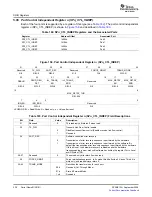
Page 206: ...R W 000 23 22 21 20 19 18 16 OUTPUT_ INPUT_ ERROR_ PORT_ MULTICAST_ PORT_ PORT_ CHECK_ Reserved DISABLE PARTICIPANT ENABLE ENABLE DISABLE R W 0 R W 0 R W 0 R W 0 R 0 R 0 15 8 Reserved R 0 7 4 3 2 1 0...

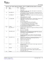
Page 207: ...ion error checking and recovery are disabled If an error condition occurs device behavior is undefined 19 MULTICAST_PARTICIPANT 0 Multicast event participant enable This read only bit is 0 to indicate...

Page 208: ...SPn_CTL Field Descriptions continued Bit Field Value Description 0 PORT_TYPE 1 Port type This read only bit indicates that the port is a serial port rather than a parallel port Serial RapidIO SRIO 208...

Page 209: ...RR_RPT_BH Address Offset 2000h 31 16 15 0 EF_PTR EF_ID R 0000h R 0007h LEGEND R Read only n Value after reset Table 150 Error Reporting Block Header Register ERR_RPT_BH Field Descriptions Bit Field Va...

Page 210: ...t To clear this bit write 0 to it 30 MSG_ERR_RSPNS Message error response endpoint device only 0 The TXU did not receive an ERROR response to a message logical layer request 1 The TXU received an ERRO...

Page 211: ...packet has not been received by an LSU or the TXU 1 An unsolicited response packet has been received by an LSU or the TXU To clear this bit write 0 to it 22 UNSUPPORTED_TRANS Unsupported transaction s...

Page 212: ...rting enable 0 Disable reporting of a message error response 1 Enable reporting of a message error response endpoint device only Save and lock transaction capture information in all Logical Transport...

Page 213: ...nsupported transaction error reporting enable 0 Disable reporting of an unsupported transaction error 1 Enable reporting of an unsupported transaction error switch or endpoint device Save and lock tra...

Page 214: ..._ADDR_CAPT Address Offset 2010h 31 0 ADDRESS_63_32 R 00000000h LEGEND R Read only n Value after reset Table 153 Logical Transport Layer High Address Capture CSR H_ADDR_CAPT Field Descriptions Bit Fiel...

Page 215: ..._31_3 Reserved XAMSBS R 0000h R 0 R 00 LEGEND R W Read Write R Read only n Value after reset Table 154 Logical Transport Layer Address Capture CSR ADDR_CAPT Field Descriptions Bit Field Value Descript...

Page 216: ...ly n Value after reset Table 155 Logical Transport Layer Device ID Capture CSR ID_CAPT Field Descriptions Bit Field Value Description 31 24 MSB_DESTID 00h FFh Most significant byte of the destinationI...

Page 217: ...only n Value after reset Table 156 Logical Transport Layer Control Capture CSR CTRL_CAPT Field Descriptions Bit Field Value Description 31 28 FTYPE 0h Fh Format type associated with the error 27 24 T...

Page 218: ...EVICEID_MSB DEVICEID R W 00h R W 00h 15 0 Reserved R 0000h LEGEND R W Read Write R Read only n Value after reset Table 157 Port Write Target Device ID CSR PW_TGT_ID Field Descriptions Bit Field Value...

Page 219: ...R W 0 LEGEND R W Read Write R Read only n Value after reset Table 159 Port Error Detect CSR n SPn_ERR_DET Field Descriptions Bit Field Value Description 31 ERR_IMP_SPECIFIC Implementation specific er...

Page 220: ...ng ackID 1 The port received a link response with an ackID that is not outstanding The capture registers do not have valid information during this error detection 4 PROTOCOL_ERROR Protocol error 0 The...

Page 221: ...GEND R W Read Write R Read only n Value after reset Table 161 Port Error Rate Enable CSR n SPn_RATE_EN Field Descriptions Bit Field Value Description 31 EN_IMP_SPECIFIC Rate counting enable for implem...

Page 222: ...ing enable for non outstanding ackIDs 0 Disable error rate counting of link responses received with an ackID that is not outstanding 1 Enable error rate counting of link responses received with an ack...

Page 223: ...Error Capture CSR 0 SPn_ERR_ATTR_CAPT_DBG0 Field Descriptions Bit Field Value Description 31 30 INFO_TYPE Type of information logged 00b Packet 01b Control symbol only error capture register 0 is vali...

Page 224: ...R_CAPT_DBG1 20CCh Port 2 SP3_ERR_CAPT_DBG1 210Ch Port 3 Figure 148 Port n Error Capture CSR 1 SPn_ERR_CAPT_DBG1 31 0 CAPTURE0 R 00000000h LEGEND R Read only n Value after reset Table 165 Port n Error...

Page 225: ...P0_ERR_CAPT_DBG2 2050h Port 0 SP1_ERR_CAPT_DBG2 2090h Port 1 SP2_ERR_CAPT_DBG2 20D0h Port 2 SP3_ERR_CAPT_DBG2 2110h Port 3 Figure 149 Port n Error Capture CSR 2 SPn_ERR_CAPT_DBG2 31 0 CAPTURE1 R 00000...

Page 226: ...P0_ERR_CAPT_DBG3 2054h Port 0 SP1_ERR_CAPT_DBG3 2094h Port 1 SP2_ERR_CAPT_DBG3 20D4h Port 2 SP3_ERR_CAPT_DBG3 2114h Port 3 Figure 150 Port n Error Capture CSR 3 SPn_ERR_CAPT_DBG3 31 0 CAPTURE2 R 00000...

Page 227: ...s Offset Associated Port SP0_ERR_CAPT_DBG4 2058h Port 0 SP1_ERR_CAPT_DBG4 2098h Port 1 SP2_ERR_CAPT_DBG4 20D8h Port 2 SP3_ERR_CAPT_DBG4 2118h Port 3 Figure 151 Port n Error Capture CSR 4 SPn_ERR_CAPT_...

Page 228: ...ent the error rate counter 01h Decrement every 1ms nominal 03h Decrement every 10ms nominal 07h Decrement every 100ms 0Fh Decrement every 1s nominal 1Fh Decrement every 10s nominal 3Fh Decrement every...

Page 229: ...alue after reset Table 175 Port Error Rate Threshold CSR n SPn_ERR_THRESH Field Descriptions Bit Field Value Description 31 24 ERROR_RATE_FAILED_THRESH These bits provide the threshold value for repor...

Page 230: ...r for 4x mode The discovery timer allows time for the link partner to enter its DISCOVERY state and if the link partner is supporting 4x mode for all 4 lanes to be aligned 0000b Reserved 0001b 0 84 ms...

Page 231: ...commodate the phase difference 27 PW_DIS Port write error reporting disable 0 Enable Port Write Error reporting default 1 Disable Port Write Error reporting 26 TGT_ID_DIS Destination ID Decode Disable...

Page 232: ...0 Four reset control symbols have not been received in a sequence 1 Four reset control symbols have been received in a sequence 1 PW_EN Port Write In Interrupt Enable If enabled the interrupt signal i...

Page 233: ...different frequencies of the DMA clock Figure 156 Port IP Prescaler Register IP_PRESCAL Address Offset 12008h 31 16 Reserved R 0000h 15 8 7 0 Reserved PRESCALE R 00h RW 0Fh LEGEND R W Read Write R Re...

Page 234: ...APT1 R 00000000h Port Write In Capture CSR 0 SP_IP_PW_IN_CAPT0 Address Offset 12018h 31 0 PW_CAPT2 R 00000000h Port Write In Capture CSR 0 SP_IP_PW_IN_CAPT0 Address Offset 1201Ch 31 0 PW_CAPT3 R 00000...

Page 235: ...Option CSR n SPn_RST_OPT 31 16 Reserved R 0000h 15 8 7 0 Reserved PORT_ID R 00h R imp LEGEND R Read only n Value after reset imp Value after reset is implementation defined Table 181 Port Reset Option...

Page 236: ...eset Table 183 Port Control Independent Register n SPn_CTL_INDEP Field Descriptions Bit Field Value Description 31 Reserved 0 This read only bit returns 0 when read 30 TX_FLW Transmit Link Flow Contro...

Page 237: ...when read 17 MAX_RETRY_EN Maximum retry error reporting enable If enabled the Port Write and interrupt are reported as errors 0b Max retry error report disable 1b Max retry error report enable 16 MAX...

Page 238: ...2 SP3_SILENCE_TIMER 14308h Port 3 Figure 160 Port Silence Timer n Register SPn_SILENCE_TIMER 31 28 27 16 SILENCE_TIMER Reserved R W Bh R 0 15 0 Reserved R 0 LEGEND R W Read Write R Read only n Value...

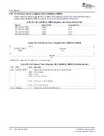
Page 239: ...Associated Port SP0_MULT_EVNT_CS 1400Ch Port 0 SP1_MULT_EVNT_CS 1410Ch Port 1 SP2_MULT_EVNT_CS 1420Ch Port 2 SP3_MULT_EVNT_CS 1430Ch Port 3 Figure 161 Port Multicast Event Control Symbol Request Regi...

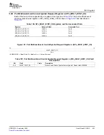
Page 240: ...2 11 0 CMD CS_EMB Reserved R W 0 R W 0 R 0 LEGEND R W Read Write R Read only n Value after reset Table 189 Port Control Symbol Transmit n Register SPn_CS_TX Field Descriptions Bit Field Value Descript...

Page 241: ...nation 156 8BNODEID field of DEVICEID_REG2 122 address MSBs for LSUn destination 155 16BIT_DEVID_LOW_BOUND field of PF_16B_CNTLn ALIGN field of SERDES_CFGRXn_CNTL 125 123 amplitude reduction de emphas...

Page 242: ...221 block 0 enable status bit 118 CNTL_SYM_UNEXPECTED_ACKID field of block 1 enable status bit 117 SPn_ERR_DET 219 block 2 enable status bit 117 command control symbol field for port n 240 block 3 en...

Page 243: ...port for source device 188 stype0 field for port n 240 data rate select field for SERDES receiver 126 stype1 field for port n 240 DEBUG field of SPn_CTL_INDEP 236 transmit request field for port n 240...

Page 244: ...cess to read only registers during boot loading device information CAR 183 113 device revision field 183 for adaptive equalizer 125 device type field 182 for entire SRIO peripheral 116 device wakeup a...

Page 245: ...SRIO peripheral block diagram 21 SPn_ERR_THRESH 229 TX FIFO bypass field for ports 231 ERROR_RATE_RECOVERY field of SPn_ERR_RATE finding interrupt source with help from interrupt status 228 decode reg...

Page 246: ...interrupt status decode registers reporting enable field 237 description 150 status field 237 introduction 97 INBOUND_ACKID field of SPn_ACKID_STAT 202 mapping example 98 INFO_TYPE field of SPn_ERR_AT...

Page 247: ...base address CSRs 191 192 register load timing diagram 37 lockout field for port n 207 register programming example 38 logical blocks of the SRIO peripheral 71 RX operation 42 logical layer TX operat...

Page 248: ...43 multiply field for SERDES PLL 131 initialization example 61 interrupting the CPU after reception 86 N order of received packets 49 next_descriptor_pointer field of RX buffer descriptor 47 order of...

Page 249: ...ut retry stopped status bit for ports 204 parameter0 control symbol field for port n 240 output swing field 128 parameter1 control symbol field for port n 240 output transmission error status bit for...

Page 250: ...f SPn_CTL 206 port write repeat period field 230 PORT_UNINITIALIZED field of SPn_ERR_STAT 203 port write request port ID 235 PORT_WIDTH_OVERRIDE field of SPn_CTL 206 port write target device ID CSR 21...

Page 251: ...enable and enable status registers 71 queue teardown bits for message transmission 168 Load Store module 43 queue transmission order 54 software shutdown details 74 R reset interrupt enable field for...

Page 252: ...le port with 1x or 4x operation 76 reporting enable field 213 small common transport system base device ID 193 status field 211 SOFT_REC field of SPn_CTL_INDEP 236 RX shared buffer SOFT field of PCR 1...

Page 253: ...out values for ports for CPPI interrupt conditions 134 136 link time out 197 for doorbell interrupt conditions 132 response time out 198 for error reset and special event port interrupt trademarks 14...

Page 254: ...ANS field of ERR_DET 210 TX_QUEUE_CNTL 0 3 174 unsupported transaction at MAU TX_QUEUE_TEAR_DOWN 168 reporting enable field 213 TX buffer descriptor fields 52 status field 211 TX buffer descriptor lin...

Page 255: ...SRIO Registers Xoff 65 Xon 65 SPRUE13A September 2006 Index 255 Submit Documentation Feedback...

Page 256: ...m TI to use such products or services or a warranty or endorsement thereof Use of such information may require a license from a third party under the patents or other intellectual property of the thir...

Reviews: