www.ti.com
LSU2
LSU4
LSU3
LSU1
MMR command
UDI
Load/Store module
RapidIO transport
and physical layers
Port x transmission
FIFO queues
TX
FIFO
RX
FIFO
Peripheral boundary
Config bus
access
Write transfer
descriptors
CPU
I/O
pins
L2 memory
= Shared resource for CPPI and MAU
Shared
TX
buffer
Shared
RX
buffer
Response
timer
Control
and
arbitrator
DMA
request
DMA
response
2.3.3.2
Direct I/O TX Operation
SRIO Functional Description
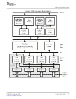
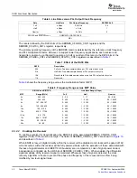
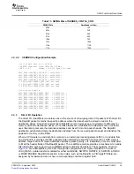
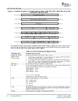
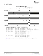
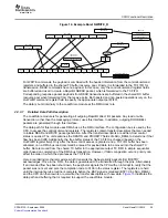
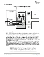
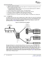
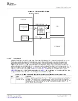
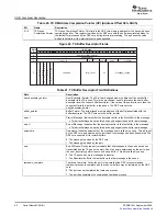
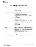
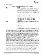
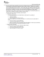
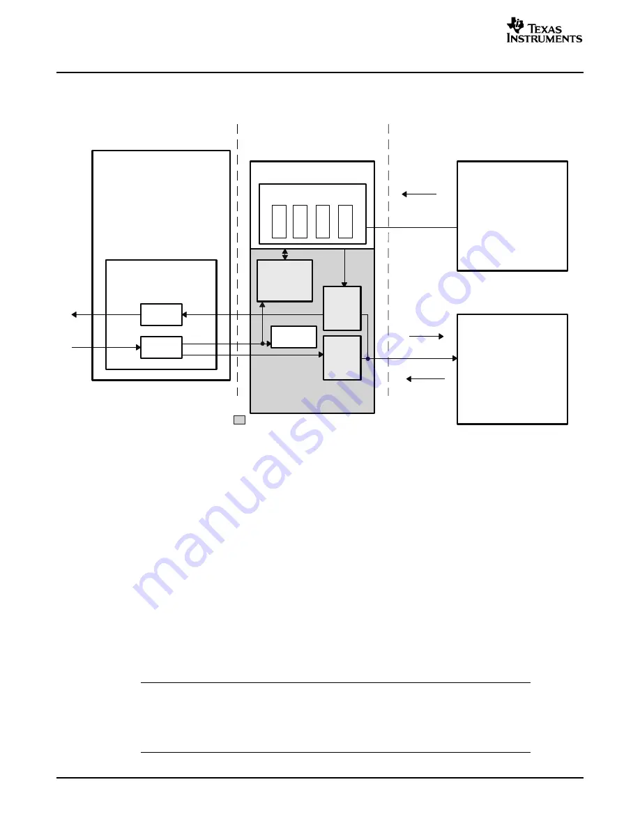
Figure 15. Load/Store Module Data Flow Diagram
WRITE Transactions:
The TX buffers are implemented in a single SRAM and shared between multiple cores. A state machine
arbitrates and assigns available buffers between the LSUs. When the DMA bus read request is
transmitted, the appropriate TX buffer address is specified within it. The data payload is written to that
buffer through the DMA bus response transaction. Depending on the architecture of the device,
interleaving of multi-segmented DMA bus responses from the DMA is possible. Upon receipt of a DMA
bus read response segment, the unit checks the completion status of the payload. Note that only one
payload can be completed in any single DMA bus cycle. The Load/Store module can only forward the
packet to the TX FIFO after the final payload byte from the DMA bus response has been written into the
shared TX buffer. Once the packet is forwarded to the TX FIFO, the shared TX buffer can be released and
made available for a new transaction.
The TX buffer space is dynamically shared among all outgoing sources, including the Load/Store module
and the TX CPPI, as well as the response packets from RX CPPI and the memory access unit (MAU).
Thus, the buffer space memory is partitioned to handle packets with and without payloads. A 4.5K-byte
buffer space is configured to support 16 packets with payloads up to 256 bytes, in addition to 16 packets
without payloads. The SRAM is configured as a 128-bit wide two port, which matches the UDI width of the
TX FIFOs.
Note:
The "UDI" ("User Defined Interface") is a reference to the interface between (a) the
SERDES and the FIFO queues and (b) the logical buffers, shared buffers, LSU and MAU
modules, response timer, and controllers (together known as the "User Application"). UDI
could also be known as the "logical/physical interface". No action is required to "define"
this interface.
40
Serial RapidIO (SRIO)
SPRUE13A – September 2006
Submit Documentation Feedback

