17
SLVSDC2B – FEBRUARY 2016 – REVISED AUGUST 2016
Product Folder Links:
Copyright © 2016, Texas Instruments Incorporated
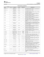
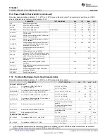
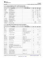
Port Data Multiplexer Switching Characteristics (continued)
Recommended operating conditions; T
A
= –40°C to +105°C unless otherwise noted
PARAMETER
TEST CONDITIONS
MIN
TYP
MAX
UNIT
(2)
See
Port Data Multiplexer USB Endpoint Requirements and Characteristics
for the USB_EP specifications.
DB1_TON
Switch-on time from enable of DEBUG path
Time from enable bit with charge
pump off
150
μ
s
Time from enable bit at charge-
pump steady state
10
DB1_TOFF
Switch-off time from disable of DEBUG path
Time from disable bit at charge-
pump steady state
500
ns
DB1_BW
3-dB bandwidth of DEBUG path
C
L
= 10 pF
200
MHz
AUX MULTIPLEXER PATH
(1)
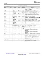
AUX_RON
On resistance of AUX_P/N to C_SBU1/2
V
i
= 3.3 V, I
O
= 20 mA
3.5
7
Ω
V
i
= 1 V, I
O
= 20 mA
2.5
5
AUX_ROND
On resistance difference between P and N paths of
AUX_P/N to C_SBU1/2
V
i
= 1 V to 3.3 V, I
O
= 20 mA
–0.25
0.25
Ω
AUX_TON
Switch-on time from enable of AUX_P/N to C_SBU1/2
Time from enable bit with charge
pump off
150
μ
s
Time from enable bit at charge-
pump steady state
15
AUX_TOFF
Switch-off time from disable of AUX_P/N to C_SBU1/2
Time from disable bit at charge-
pump steady state
500
ns
AUX_BW
3-dB bandwidth of AUX_P/N to C_SBU1/2 path
C
L
= 10 pF
200
MHz
USB_RP MULTIPLEXER PATH
(1) (2)
USB_RON
On resistance of USB_RP to C_USB_TP/TN/BP/BN
V
i
= 3 V, I
O
= 20 mA
4.5
10
Ω
V
i
= 400 mV, I
O
= 20 mA
3
7
USB_ROND
On resistance difference between P and N paths of
USB_RP to C_USB_TP/TN/BP/BN
V
i
= 0.4 V to 3 V, I
O
= 20 mA
–0.15
0.15
Ω
USB_TON
Switch-on time from enable of USB USB_RP path
Time from enable bit with charge
pump off
150
µs
Time from enable bit at charge-
pump steady state
15
USB_TOFF
Switch-off time from disable of USB_RP path
Time from disable bit at charge-
pump steady state
500
ns
USB_BW
3-dB bandwidth of USB_RP path
C
L
= 10 pF
850
MHz
USB_ISO
Off isolation of USB_RP path
R
L
= 50
Ω
, V
I
= 800 mV, f = 240
MHz
–19
dB
USB_XTLK
Channel to channel crosstalk of USB_RP path
R
L
= 50
Ω
, f = 240 MHz
–26
dB
C_SBU1/2 OUTPUT
R_SBU_OPEN
Resistance of the open C_SBU1/2 paths
V
i
= 0 V to LDO_3V3
1
M
Ω
R_USB_OPEN
Resistance of the open C_USB_T/B/P/N paths
V
i
= 0 V to LDO_3V3
1
M
Ω
(1)
The TCLMP_PRT time includes the time through the digital synchronizers. When the clock speed is reduced, the signal assertion time
may be longer.
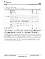
7.13 Port Data Multiplexer Clamp Characteristics
Recommended operating conditions; T
A
= –40°C to +105°C unless otherwise noted
PARAMETER
TEST CONDITIONS
MIN
TYP
MAX
UNIT
VCLMP_IND
Clamp voltage triggering indicator to digital core
3.8
3.95
4.1
V
ICLMP_IND
Clamp current at VCLMP_IND
10
250
μ
A
TCLMP_PRT
(1)
Time from clamp current crossing ICLMP_IND to
interrupt signal assertion
I
≥
ICLMP_IND rising
0
4
μ
s
ICLMP
USB_EP and USB_RP port clamp current
V = LDO_3V3
250
nA
V = VCL 500 mV
3.5
15
mA

