Time (500
P
s/div)
Cu
rr
en
t (
A)
Volt
ag
e
(V)
-1
-1
0
0
1
1
2
2
3
3
4
4
5
5
6
6
D010
I CC2
C_CC2
PP_CABLE
Time (10
P
s/div)
Cu
rr
en
t (
A)
Volt
ag
e
(V)
0
-4
1
-2
2
0
3
2
4
4
5
6
6
8
7
10
D009
I CC2
C_CC2
PP_CABLE
47
SLVSDC2B – FEBRUARY 2016 – REVISED AUGUST 2016
Product Folder Links:
Copyright © 2016, Texas Instruments Incorporated
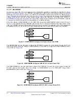
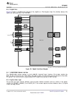
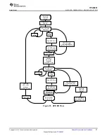
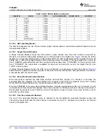
9.3.3.22 PP_CABLE to C_CC1 and C_CC2 Switch Architecture
shows the switch architecture for the PP_CABLE switch path to the C_CCc pins. Each path provides a
unidirectional current from PP_CABLE to C_CC1 and C_CC2. The switch structure blocks reverse current from
C_CC1 or C_CC2 to PP_CABLE.
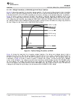
9.3.3.23 PP_CABLE to C_CC1 and C_CC2 Current Limit
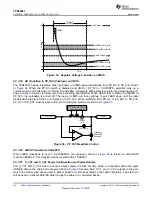
The PP_CABLE to C_CC1 and C_CC2 share current limiting through a single FET on the PP_CABLE side of the
switch. The current limit ILIMPPCC is adjustable between two levels. When the current exceeds ILIMPPCC, the
current-limit circuit activates. Depending on the severity of the over-current condition, the transient response will
react in one of two ways:
and
show the approximate response time and clamping
characteristics of the circuit for a hard short while
shows the approximate response time and clamping
characteristics for a soft short. The switch does not have reverse current blocking when the switch is enabled
and current is flowing to either C_CC1 or C_CC2.
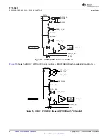
Figure 40. PP_CABLE to C_CCn Current Limit With a Hard Short
Figure 41. PP_CABLE to C_CCn Current Limit With a Hard Short (Extended Time Base)


