6
SLVSDC2B – FEBRUARY 2016 – REVISED AUGUST 2016
Product Folder Links:
Copyright © 2016, Texas Instruments Incorporated
Pin Functions (continued)
PIN
CATEGORY
I/O TYPE
POR STATE
DESCRIPTION
NAME
NO.
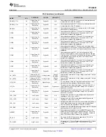
PP_HV
33
High Current
Power
N/A
HV supply for VBUS. Bypass with capacitance CPP_HV to GND.
Tie pin to GND when unused
34
R_OSC
52
Digital Core I/O
and Control
Analog I/O
Hi-Z
External resistance setting for oscillator accuracy. Connect
R_OSC to GND through resistance RR_OSC.
RESETZ
21
Digital Core I/O
and Control
Digital I/O
Push-Pull
Output (Low)
General-purpose digital I/O 9. Active low reset output when
VIN_3V3 is low (driven low on start-up). Float pin when unused.
RPD_G1
12
Type-C Port
Analog I/O
Hi-Z
Tie pin to C_CC1 when configured to receive power in dead-
battery or no-power condition. Tie pin to GND otherwise.
RPD_G2
16
Type-C Port
Analog I/O
Hi-Z
Tie pin to C_CC2 when configured to receive power in dead-
battery or no-power condition. Tie pin to GND otherwise.
SENSEN
29
External HV FET
Control and Sense
Analog Input
Analog Input
Positive sense for external high voltage power path current sense
resistance. Short pin to VBUS when unused.
SENSEP
30
External HV FET
Control and Sense
Analog Input
Analog Input
Positive sense for external high voltage power path current sense
resistance. Short pin to VBUS when unused.
SPI_CLK
37
Digital Core I/O
and Control
Digital Output
Digital Input
SPI serial clock. Connect pin directly to SPI Flash IC. Refer to the
Boot Code
section for more details on the SPI Flash.
SPI_MISO
35
Digital Core I/O
and Control
Digital Input
Digital Input
SPI serial master input from slave. Tie pin to LDO_3V3 through a
3.3-k
Ω
resistor.
SPI_MOSI
36
Digital Core I/O
and Control
Digital Output
Digital Input
SPI serial master output to slave. Connect pin directly to SPI flash
IC.
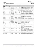
SPI_SSZ
39
Digital Core I/O
and Control
Digital Output
Digital Input
SPI slave select. Tie pin to LDO_3V3 through a 3.3-k
Ω
resistor.
SS
3
External HV FET
Control and Sense
Analog Output
Driven Low
Soft Start. Tie pin to capacitance CSS to ground.
SWD_CLK
50
Port Multiplexer
Digital Input
Resistive Pull
High
SWD serial clock. Float pin when unused.
SWD_DATA
49
Port Multiplexer
Digital I/O
Resistive Pull
High
SWD serial data. Float pin when unused.
USB_RP_N
5
Port Multiplexer
Analog I/O
Hi-Z
System-side USB2.0 high-speed connection to the port
multiplexer. Ground pin with between 1-k
Ω
and 5-M
Ω
resistance
when unused.
USB_RP_P
4
Port Multiplexer
Analog I/O
Hi-Z
System-side USB2.0 high-speed connection to the port
multiplexer. Ground pin with between 1-k
Ω
and 5-M
Ω
resistance
when unused.
VBUS
17
High Current
Power
N/A
5-V output from PP_5V0. Input or output from PP_HV up to 20 V.
Bypass with capacitance CVBUS to GND.
18
VDDIO
42
Low Current
Power
N/A
VDD for I/O. Some I/Os are reconfigurable to be powered from
VDDIO instead of LDO_3V3. When VDDIO is not used, tie pin to
LDO_3V3. When not tied to LDO_3V3 and used as a supply
input, bypass with capacitance CVDDIO to GND.
VIN_3V3
53
Low Current
Power
N/A
Supply for core circuitry and I/O. Bypass with capacitance
CVIN_3V3 to GND.
GND (Thermal Pad)
Ground
Ground
Hi-Z
Ground. Connect directly to ground plane in accordance with the
guidelines listed in the
Layout Guidelines
section to achieve the
measured values in the
Thermal Information
table.


