VBUS
CC1/2
SSTX1/RX1
SSTX2/RX2
USB2.0
Type-C
Receptacle
TPS65981
(Dock or Monitor)
VBUS
CC1/2
USB2_UP
USB Billboard
USB2_DN1
USB2_DN4
USB3_UP
USB3_DN1
SBU
AUX_P/N
USB_RP
PP_HV
VIN_3V3
PP_CABLE
SBU1/2
D+/D-
DisplayPort
(Receptacle
or Scalar)
HD3SS460
(SS MUX)
TUSB8041
(USB Hub)
AM
S
EL
P
O
L
EN
2 or 4 Lane DP
SSTX/RX
USB3
SSTX/RX
SBU1/2
ML0 – ML3
SSTX/RX
GPIO
0
DEBUG1
GPIO
3
GPIO2
ML0 – ML3
USB2.0
Endpoint
HPD
GPIO4
Type-A
USB3
Receptacle
Barrel Jack
System Power
Receptacle
Buck Regulator
Buck Regulator
VIN
VOUT
VOUT
5 V, 500 mA
3.3 V, 50 mA
VIN
VIN
1.8 V
R1
R2
VOUT
20 V
20 V, 4 A
4-20 V
HV_GA
TE1
HV_GA
TE2
SENSEP
CSD87501L
SENSEN
GPIO7
PDO3
GPIO6
PDO2
GPIO8
PDO4
DBG_CTL1
EN
20 V
5/9/15/20 V, 3 A
Buck Regulator
Variable
Copyright © 2016, Texas Instruments Incorporated
78
SLVSDC2B – FEBRUARY 2016 – REVISED AUGUST 2016
Product Folder Links:
Copyright © 2016, Texas Instruments Incorporated
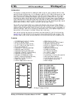
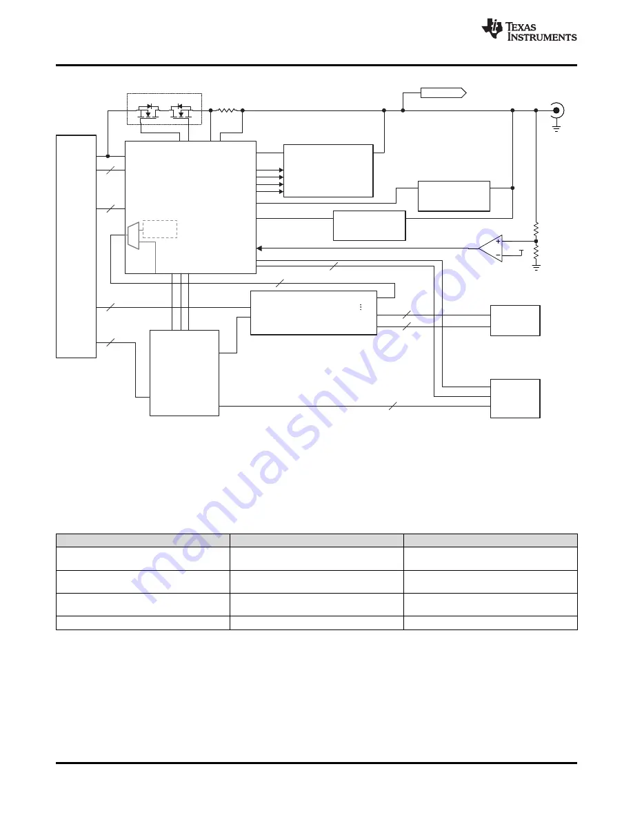
Figure 76. Type-C and PD Dock or Monitor Application
10.2.2.1 Design Requirements
For a USB Type-C and PD dock application,
shows the input/output voltage requirements and expected
current capabilities for the TPS65981
Table 12. Dock Application Design Parameters
DESIGN PARAMETER
EXAMPLE VALUE
DIRECTION OF CURRENT
PP_CABLE Input Voltage and Current
Capabilities
5 V, 500 mA
Sourcing to VCONN (CC2 or CC1)
PP_HV Output Voltage and Current
Capabilities
5V/9V/15V/20 V, 3 A
Sourcing to VBUS
PP_EXT Input Voltage and Current
Capabilities
12-20 V, 5 A
Sinking from VBUS
VIN_3V3 Voltage and Current Requirements
2.85 - 3.45 V, 50 mA
Internal TPS65981 Circuitry
10.2.2.2 Detailed Design Procedure
The same passive components used in the are also applicable in this design to support all of the features of the
TPS65981. Additional design information is provided below for changes in passive components required by the
dock or monitor application. The TPS65981 control of the HD3SS460 SuperSpeed multiplexer is explained in
HD3SS460 Control and DisplayPort Configuration
.


