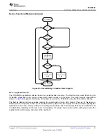
CC1
VBUS
Type-C
Plug Event
Active
TPS65981
Code
BOOT
PD Contract
Accept
PS_Ready
DP Alt.
Mode
20V, 3 A
APPLICATION
0 V
0 V
0 V
5 V
20 V
20 V
3.3 V
1.67 V
(Barrel Jack)
Ext. Power
VOUT Var. Buck
Barrel Jack
Detect GPIO
(DBG_CTL1)
Buck EN
PDO4
(GPIO8)
(PP_HV)
Barrel Jack
Plug Event
81
SLVSDC2B – FEBRUARY 2016 – REVISED AUGUST 2016
Product Folder Links:
Copyright © 2016, Texas Instruments Incorporated
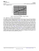
10.2.2.3 Application Curves
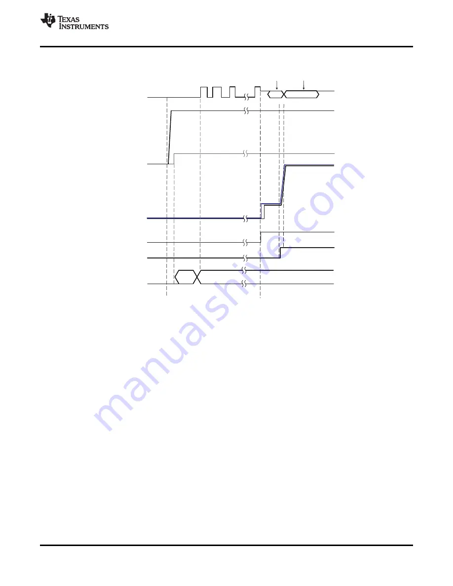
Figure 79. TPS65981 Variable Buck Regulator in Dock or Monitor Application Timing Diagram
11 Power Supply Recommendations
11.1 3.3 V Power
11.1.1 VIN_3V3 Input Switch
The VIN_3V3 input is the main supply to the TPS65981. The VIN_3V3 switch (S1 in
) is a unidirectional
switch from VIN_3V3 to LDO_3V3, not allowing current to flow backwards from LDO_3V3 to VIN_3V3. This
switch is on when 3.3 V is available. See
for the recommended external capacitance on the VIN_3V3
pin.
11.1.2 VBUS 3.3-V LDO
The 3.3 V LDO from VBUS steps down voltage from VBUS to LDO_3V3. This allows the TPS65981 to be
powered from VBUS when VIN_3V3 is not available. This LDO steps down any recommended voltage on the
VBUS pin. When VBUS is 20 V, as is allowable by USB PD, the internal circuitry of the TPS65981 will operate
without triggering thermal shutdown; however, a significant external load on the LDO_3V3 pin may increase
temperature enough to trigger thermal shutdown. The VBUS 3.3-V LDO blocks reverse current from LDO_3V3
back to VBUS allowing VBUS to be unpowered when LDO_3V3 is driven from another source. See
for
the recommended external capacitance on the VBUS and LDO_3V3 pins.
11.2 1.8 V Core Power
Internal circuitry is powered from 1.8 V. There are two LDOs that step the voltage down from LDO_3V3 to 1.8 V.
One LDO powers the internal digital circuits. The other LDO powers internal low voltage analog circuits.

