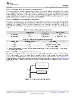
PP_5V0
VBUS
Fast
current
limit
PP_5V0 Gate Control
and Current Limit
PP_HV
Fast
current
limit
PP_HV Gate Control
and Current Limit
HV Gate Control and Sense
SENSEP
SENSEN
HV_GA
TE1
HV_GA
TE2
PP_EXT
AGND
Copyright © 2016, Texas Instruments Incorporated
83
SLVSDC2B – FEBRUARY 2016 – REVISED AUGUST 2016
Product Folder Links:
Copyright © 2016, Texas Instruments Incorporated
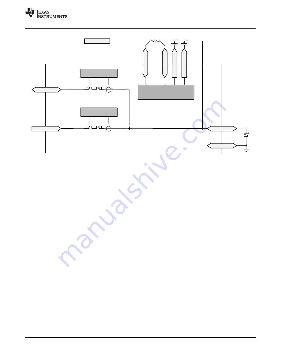
Figure 80. Schottky on VBUS for Current Surge Protection
12 Layout
12.1 Layout Guidelines
Proper routing and placement will maintain signal integrity for high-speed signals and improve the thermal
dissipation from the TPS65981 power path. The combination of power and high-speed data signals are easily
routed if the following guidelines are followed. Consult with a printed circuit board (PCB) manufacturer to verify
manufacturing capabilities.
12.1.1 TPS65981 Recommended Footprint
shows the TPS65981 footprint with 56 0.6-mm long by 0.25-mm wide rectangular pads and 1 5.9-mm
by 5.9-mm square, grounded Thermal Pad. This footprint is applicable to boards that will be using a non-HDI
process using all through-hole vias or an HDI PCB process using smaller vias to fan-out into the inner layers of
the PCB. Via fills and via tenting is recommended for size-constrained applications. The footprint allows for easy
fan-out into other layers of the PCB and thermal dissipation into the GND plane(s) from vias placed directly under
the large, square grounded Thermal Pad.
shows the minimum recommended via sizing for use under
the thermal pad. The size is 8-mil hole and 16-mil diameter. This via size will allow for approximately 1.8-A of DC
current rating at 1.5 m
Ω
of resistance with 1.3 nH of inductance. Some board manufacturers can guarantee vias
with a 6-mile hole and 12-mil diameter using a standard mechanical drill. TI recommends to verify these numbers
with board manufacturing processes used in fabrication of the PCB. This footprint is available for download on
the TPS65981 product folder on the
.


