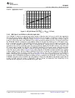
SWD_CLK
SWD_DATA
LDO_3V3
SWD_RPU
SWDCLKin
LDO_3V3
SWDIOin
CMOS
Output
SWDIOout
SWD_OE
SWD_RPU
64
SLVSDC2B – FEBRUARY 2016 – REVISED AUGUST 2016
Product Folder Links:
Copyright © 2016, Texas Instruments Incorporated
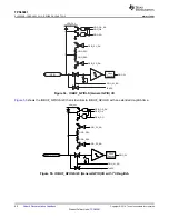
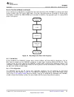
9.3.17.6 IOBUF_GPIOHSSWD
shows the I/O buffers for the SWD interface. The CLK input path is a comparator with a pull-up
SWD_RPU on the pin. The data I/O consists of an identical input structure as the CLK input but with a tri-state
CMOS output driver.
Figure 60. IOBUF_GPIOHSSWD
9.3.18 Thermal Shutdown
The TPS65981 has both a central thermal shutdown to the chip and a local thermal shutdown for the power path
block. The central thermal shutdown monitors the temperature of the center of the die and disables all functions
except for supervisory circuitry and halts digital core when die temperature goes above a rising temperature of
TSD_MAIN. The temperature shutdown has a hysteresis of TSDH_MAIN and when the temperature falls back
below this value, the device resumes normal operation. The power path block has a local thermal-shutdown
circuit to detect an over temperature condition because of over current and quickly turn off the power switches.
The power path thermal shutdown values are TSD_PWR and TSDH_PWR. The output of the thermal-shutdown
circuit is de-glitched by TSD_DG before triggering. The thermal-shutdown circuits interrupt to the digital core.
9.3.19 Oscillators
The TPS65981 has two independent oscillators for generating internal clock domains. A 48-MHz oscillator
generates clocks for the core during normal operation and clocks for the USB 2.0 endpoint physical layer. An
external resistance is placed on the R_OSC pin to set the oscillator accuracy. A 100-kHz oscillator generates
clocks for various timers and clocking the core during low-power states.
9.4 Device Functional Modes
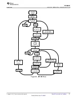
9.4.1 Boot Code
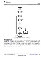
The TPS65981 has a Power-on-Reset (POR) circuit that monitors LDO_3V3 and issues an internal reset signal.
The digital core, memory banks, and peripherals receive clock and RESET interrupt is issued to the digital core
and the boot code starts executing.
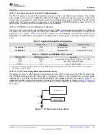
provides the TPS65981 boot code sequence.
The TPS65981 boot code is loaded from OTP on POR, and begins initializing TPS65981 settings. This
initialization includes enabling and resetting internal registers, loading trim values, waiting for the trim values to
settle, and configuring the device I
2
C addresses.
The unique I
2
C address is based on the digital input read on the DEBUG_CTL1/2 pins, which can be tied to GND
through a pull-down resistor or to LDO_3V3 through a pull-up resistor.


