Write Mode
CKPH – 1, CKPL – 0 (MSP430)
Data Transition – SCLK Falling Edge
MOSI Valid – SCLK Rising Edge
Switch
SCLK
Polarity
Read Mode
CKPH – 0, CKPL – 0 (MSP430)
Data Transition – SCLK Rising Edge
MISO Valid – SCLK Falling Edge
Single Read Operation
SCLK
MOSI
MISO
SS*
Write Address Byte
Read Data Byte
B7
B7
B6
B6
B5
B5
B4
B4
B3
B3
B2
B2
B1
B1
B0
B0
Don't Care
No Data Transitions (All High/Low)
SLOU186F
–
AUGUST 2006
–
REVISED AUGUST 2010
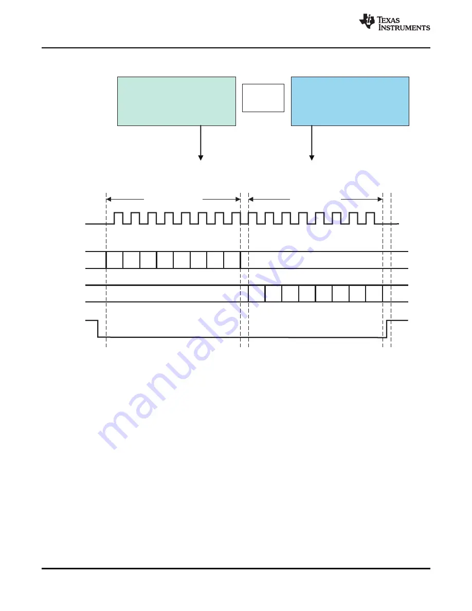
The SPI read operation is shown in
Figure 5-10. Serial
–
SPI Interface Communication (Read Mode)
The read command is sent out on the MOSI pin, MSB first, in the first eight clock cycles. MOSI data
changes on the falling edge, and is validated in the reader on the rising edge, as shown in
.
During the write cycle, the serial data out (MISO) is not valid. After the last read command bit (B0) is
validated at the eighth rising edge of SCLK, after half a clock cycle, valid data can be read on the MISO
pin at the falling edge of SCLK. It takes eight clock edges to read out the full byte (MSB first).
Note:
When using the hardware SPI (for example, an MSP430 hardware SPI) to implement the foregoing
feature, care must be taken to switch the SCLK polarity after write phase for proper read operation.
The example clock polarity for the MSP430-specific environment is shown in the write-mode and
read-mode boxes of
. See the USART-SPI chapter for any specific microcontroller family
for further information on the setting the appropriate clock polarity.
This clock polarity switch must be done for all read (single, continuous) operations.
The MOSI (serial data out) should not have any transitions (all high or all low) during the read cycle. Also,
the SS* should be low during the whole write and read operation.
The continuous read operation is illustrated in
42
System Description
Copyright
©
2006
–
2010, Texas Instruments Incorporated
focus.ti.com:


