8 (Parallel)
3 (SPI)
Z – Matching
Circuit
Tx_Out
Rx_IN1
Rx_IN2
VDD_X
VDD_I/O
SYS_CLK
DATA_CLK
VDD
TRF796x
MSP430
Xtal
13.56 MHz
IRQ
Xtal In
Xtal Out
SLOU186F
–
AUGUST 2006
–
REVISED AUGUST 2010
2
Description (continued)
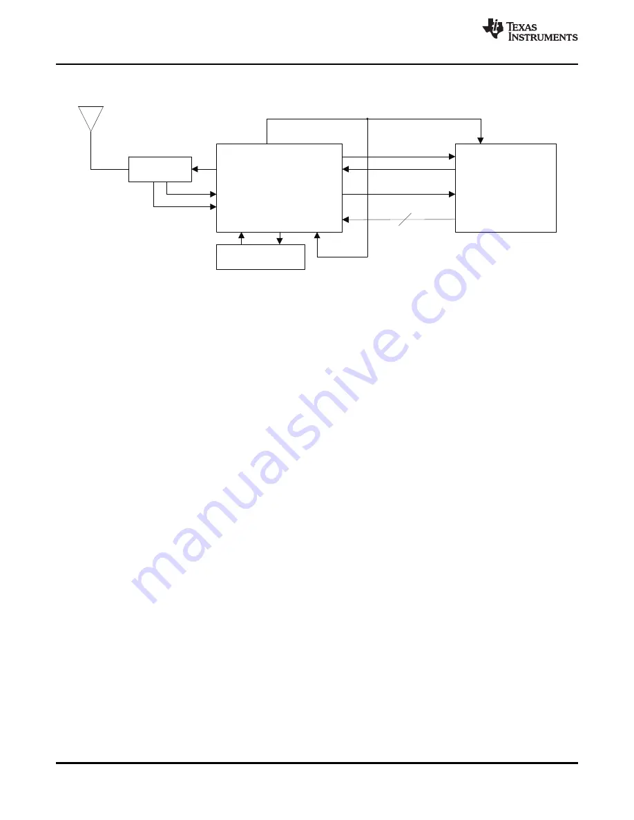
Figure 2-1. Typical Application
A parallel or serial interface can be implemented for communication between the MCU and reader.
Transmit and receive functions use internal encoders and decoders with a 12-byte FIFO register. For
direct transmit or receive functions, the encoders / decoders can be bypassed so the MCU can process
the data in real time. The transmitter has selectable output power levels of 100 mW (20 dBm) or 200 mW
(23 dBm) into a 50-
Ω
load (5 -V supply) and is capable of ASK or OOK modulation. Integrated voltage
regulators ensure power-supply noise rejection for the complete reader system.
Data transmission comprises low-level encoding for ISO15693, modified Miller for ISO14443-A,
high-bit-rate systems for ISO14443 and Tag-it coding systems. Included with the data encoding is
automatic generation of SOF, EOF, CRC, and / or parity bits.
The receiver system enables AM and PM demodulation using a dual-input architecture. The receiver also
includes an automatic gain control option and selectable gain. Also included is a selectable bandwidth to
cover a broad range of input sub-carrier signal options. The received signal strength for AM and PM
modulation is accessible via the RSSI register. The receiver output is a digitized sub-carrier signal among
a selectable protocol and bit rate as outlined in
. A selected decoder delivers bit stream and a
data clock as outputs.
The receiver system also includes a framing system. This system performs CRC and / or parity check,
removes the EOF and SOF settings, and organizes the data in bytes. Framed data is then accessible to
the MCU via a 12-byte FIFO register and MCU interface. The framing supports ISO14443 and ISO15693
protocols.
The TRF7960/61 supports data communication levels from 1.8 V to 5.5 V for the MCU I/O interface, while
also providing a data synchronization clock. An auxiliary 20-mA regulator (pin 32) is available for
additional system circuits.
4
Description (continued)
Copyright
©
2006
–
2010, Texas Instruments Incorporated
focus.ti.com:


