


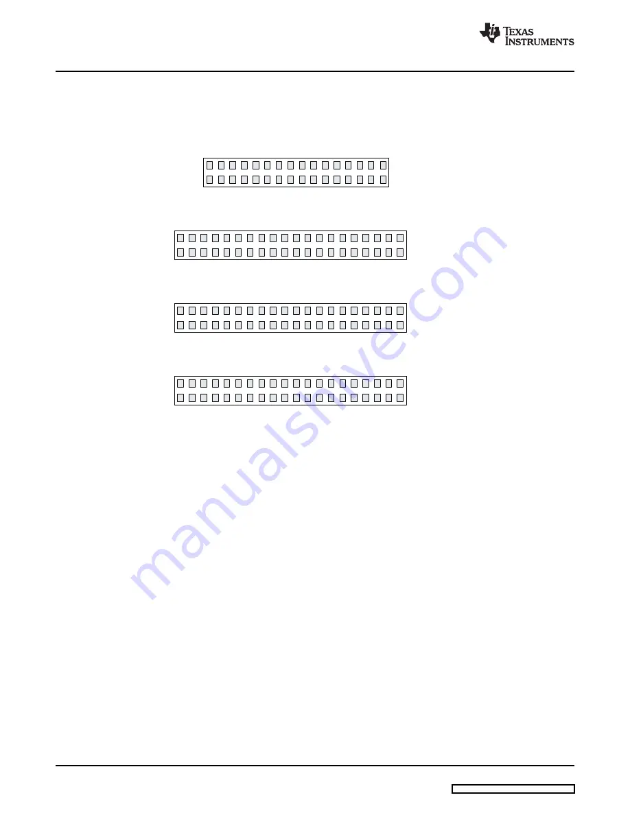
GND
GND
GND
GND
CLK
NC
D1
D2
D4
D3
D5
D6
D7
D8
D9
D10
D1
1
D12
D13
D14
D15
D0
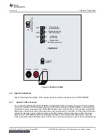
J18 Channel 5
J19 Channel 6
J20 Channel 7
J21 Channel 8
J5 Channel 2
J4 Channel 3
J6 Channel 4
J3 Channel 1
CLK
NC
D1
D2
D4
D3
D5
D6
D7
D8
D9
D10
D1
1
D12
D13
D0
NC
NC
CLK
NC
D1
D2
D4
D3
D5
D6
D7
D8
D9
D10
D1
1
D12
D13
D0
NC
NC
NC
NC
CLK
NC
D1
D2
D4
D3
D5
D6
D7
D8
D9
D10
D1
1
D12
D13
D0
NC
NC
NC
NC
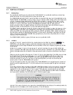
3.6
USB I/O Connection
4
Software Installation
Software Installation
www.ti.com
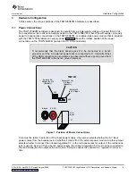
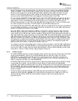
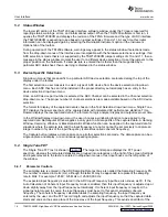
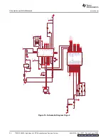
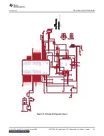
For the current release, four of the header posts are enabled for serial data formats. For up to
four-channel ADCs, the parallel deserialized sample data is presented on the corresponding output
header. For eight-channel serial data formats, the TSW1200 user interface software selects whether to
output the lower four channels of data on the output headers for Channels 1 through 4 or whether to
output the data for Channels 5 through 8 on the output headers for Channels 1 through 4. Output headers
for Channels 5 through 8 are unused for this release.
Figure 6. Pinout of Header Posts for Parallel Output Data
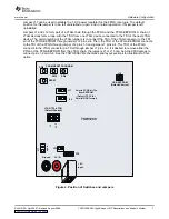
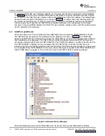
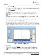
Control of the TSW1200EVM is through a USB connection to a PC running Windows operating system.
For the computer, the drivers needed to access the USB port are included on the TSW1200 Installation
CD and are installed during the installation process. The USB is accessed as a virtual communication port
(VCP) and shows up in the Hardware Device Manager as TSW1200 under COM ports and as TSW1200
EVM under Multi-Port Serial Adapters. See Figure 8. On the TSW1200EVM, the USB port acts as a bridge
to UART control of the FPGA. Control of the FPGA is managed by reads and writes to a register map of
control registers defined in the design of the FPGA. Normally, register writes from the TSW1200 user
interface software sets up the mode of operation of the FPGA. These register writes define such things as
the depth of FIFO to use for data capture or from which channel of an ADC to capture data. Then, a single
register access triggers the filling of the capture FIFOs. Immediately after the capture FIFOs have
captured the desired amount of data, the FIFO data is streamed back up the USB connection to the
TSW1200 user interface software. The UART data rate between the FPGA and the USB port can be set
to 115K, 230K, or 460K baud. A UART baud rate of 920K is not recommended for reliable data transfer.
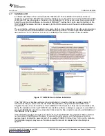
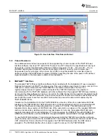
On first connection of the USB port to a computer, the Microsoft Found New Hardware Wizard appears.
Follow the dialog box prompts as covered in the Software Installation section of this User’s Guide.
TSW1200EVM: High-Speed LVDS Deserializer and Analysis System
12
SLAU212A – April 2007 – Revised August 2008


