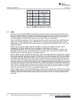


5.1.2
Instrument Options
5.1.3
Data Capture Options
5.1.4
Test Options
www.ti.com
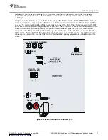
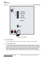
User Interface
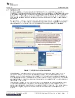
The Instrument Options menu tab contains two options: Reinitialize Instrument and Read ADC EVM Setup
Procedure.
The Reinitialize Instrument option causes the TSW1200 software to reset itself to initial conditions and to
read the firmware settings from the TSW1200EVM again. The firmware and software revisions then are
displayed in the status window. This command is useful for cases where the jumper settings on the
TSW1200EVM may have changed since the TSW1200 software was opened, or in cases where the USB
connection to the PC has been dropped and the COM port must be reopened.
The Read ADC EVM Setup Procedure command causes the TSW1200 software to read a comment string
from the ini file for the ADC that is currently selected and then display that comment string in the status
pane. This comment string generally contains necessary setup information pertaining to the ADC EVM,
such as possibly requiring a non-default data format or required jumper setting for the EVM to
communicate properly with the TSW1200EVM.
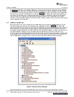
The Data Capture menu tab contains two options: Capture Options and UART Baud Rate.
Capture Options allows for continuous capture that can be checked or unchecked. Continuous capture
causes the capture button to continuously capture, process, and display test data. Once the results are
displayed, the capture process automatically begins again at the desired capture interval The default
capture interval is zero, which means that the next capture is started once the current results are
displayed. The capture interval can be set in seconds to make the continuous capture less frequent.
The UART baud rate can be set to one of four data rates. This controls the data rate of unloading the
FIFO capture from the TSW1200EVM FPGA to the USB port. The UART baud rate is the limiting factor for
the time it takes to capture long record lengths of data. The UART data rate is commonly set to 460800,
as 921600 is not recommended for reliable data transfer.
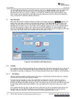
The Test Options menu tab allows for setting the parameter options for the Single Tone FFT test and the
Time Domain test. Later revisions of the TSW1200 software will allow for setting test parameters for a
Dual Tone FFT test and the ACPR test.
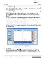
For a Single Tone FFT test, the RMS line may be enabled or disabled. When enabled, a horizontal marker
is displayed over the FFT plot to indicate the RMS average of the noise floor of the FFT plot. The RMS
average is computed over all of the FFT bins except the bin containing the input frequency. More
precisely, the RMS line = SINAD + FFT Record Length Process Gain where FFT Record Process Gain =
10log(number of points/2).
SNR, SFDR, and SINAD can be expressed in either dBc or dBFS as selected by the dBFS selection
under the Single Tone FFT options.
By default, the noise calculations for SNR and SINAD do not include the five FFT bins around the
expected input frequency or the first five FFT bins at DC. The rest of the FFT bins out to the Nyquist
frequency are included in the calculation of the total noise. Vertical marker cursors are present in the FFT
display that indicate the beginning and the end of the bandwidth of interest for noise calculations. Because
these vertical markers are located at the extreme left-most and right-most positions on the FFT display,
these vertical markers often are not noticeable. It is possible to compute the total noise power over a
narrower range than the default DC through Nyquist band of frequencies. An integration band for the noise
calculations can be set in two ways. First, the mouse can be used to click on one of the vertical cursors
and drag it to a new desired location. Second, the Cursor Band Location window under the Single Tone
FFT Test Option in the tool bar can be used to set a new frequency band of integration for the calculation
of the total noise power.
Also excluded from calculation of the SNR is the power in the first five harmonics of the input frequency.
These first five harmonics are included in calculation of SINAD (signal to noise and distortion) and thus
this is the principal difference between SNR and SINAD. (SINAD is sometimes called SNDR, signal to
noise and distortion ratio.) The number of harmonics to exclude from SNR can be set to a value other than
the default 5 in the Number of Harmonics window in the Single Tone FFT Test Option in the toolbar.
SLAU212A – April 2007 – Revised August 2008
TSW1200EVM: High-Speed LVDS Deserializer and Analysis System
17