
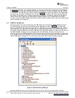


7
Schematics and Bill of Materials
7.1
Schematics
+6V_IN
6V_IN
INHIBIT
+3.3V
+2.5V
+1.2V
+3.3V
+2.5V
+1.2V
VCC_BANK5_ADJ
+1.8V
VCC_BANK5_ADJ
+6V
+3.3V_USB
+6V
+6V
+5V
ADC
+6V
GND
GND
GND
GND
GND
GND
GND
GND
GND
GND
GND
GND
GND
GND
GND
GND
GND
GND
GND
GND
GND
GND
GND
GND
GND
GND
+6V
+3.3V
GND
+3.3V_USB
+1.2V
GND
GND
+3.3V_USB
GND
+3.3V_USB
+5V
ADC
VCC_BANK5_ADJ
+6V
+2.5V
JP8default:Short1-2
J22default:Shorted
J17default:OPEN
C82
2.2uF
C82
2.2uF
1
2
C64
.01uF
C64
.01uF
1
2
C20
.01uF
C20
.01uF
1
2
R49
33.2K
R49
33.2K
C33
10uF
10%
16V
C33
10uF
10%
16V
1
2
C37
.1uF
C37
.1uF
1
2
J14
BANANA_JACK_BLK
J14
BANANA_JACK_BLK
C67
.1uF
10%
16V
C67
.1uF
10%
16V
1
2
U9
TPS76750QPWP
U9
TPS76750QPWP
GND/HTSNK2
2
NC3
17
GND
3
NC1
4
EN
5
IN1
6
NC2
8
GND/HTSNK5
1
1
GND/HTSNK1
1
GND/HTSNK3
9
OUT1
13
GND/HTSNK4
10
IN2
7
RESET
16
GND/HTSNK6
12
OUT2
14
FB/NC
15
NC4
18
GND/HTSNK7
19
GND/HTSNK8
20
PWRP
AD
21
C89
10uF
10%
16V
C89
10uF
10%
16V
1
2
C32
.1uF
10%
16V
C32
.1uF
10%
16V
1
2
C12
.01uF
C12
.01uF
1
2
C63
.1uF
C63
.1uF
1
2
C19
.1uF
C19
.1uF
1
2
+
C101
47uF
10V
20%
+
C101
47uF
10V
20%
C84
2.2uF
C84
2.2uF
1
2
C36
.01uF
C36
.01uF
1
2
C7
.1uF
C7
.1uF
1
2
+
C102
10uF
16V
10%
LOWESR
+
C102
10uF
16V
10%
LOWESR
C35
.1uF
C35
.1uF
1
2
R59
10K
R59
10K
U1
1
TPS76733QPWP
U1
1
TPS76733QPWP
GND/HTSNK2
2
NC3
17
GND
3
NC1
4
EN
5
IN1
6
NC2
8
GND/HTSNK5
1
1
GND/HTSNK1
1
GND/HTSNK3
9
OUT1
13
GND/HTSNK4
10
IN2
7
RESET
16
GND/HTSNK6
12
OUT2
14
FB/NC
15
NC4
18
GND/HTSNK7
19
GND/HTSNK8
20
PWRP
AD
21
C8
.01uF
C8
.01uF
1
2
C62
.01uF
C62
.01uF
1
2
+
C51
47uF
10V
20%
+
C51
47uF
10V
20%
R50
30.1K
R50
30.1K
U12
TPS76701QPWP
U12
TPS76701QPWP
GND/HTSNK2
2
NC3
17
GND
3
NC1
4
EN
5
IN1
6
NC2
8
GND/HTSNK5
1
1
GND/HTSNK1
1
GND/HTSNK3
9
OUT1
13
GND/HTSNK4
10
IN2
7
RESET
16
GND/HTSNK6
12
OUT2
14
FB/NC
15
NC4
18
GND/HTSNK7
19
GND/HTSNK8
20
PWRP
AD
21
C15
.1uF
C15
.1uF
1
2
C61
.1uF
C61
.1uF
1
2
+
C96
47uF
10V
20%
+
C96
47uF
10V
20%
R45
100K
R45
100K
+
C103
10uF
16V
10%
LOWESR
+
C103
10uF
16V
10%
LOWESR
R51
100K
R51
100K
C60
.01uF
C60
.01uF
1
2
C59
.1uF
C59
.1uF
1
2
C18
.01uF
C18
.01uF
1
2
+
C108
100uF
16V
20%
+
C108
100uF
16V
20%
C55
.1uF
C55
.1uF
1
2
+
C97
47uF
10V
20%
+
C97
47uF
10V
20%
C58
.01uF
C58
.01uF
1
2
C1
1
.1uF
C1
1
.1uF
1
2
68OHM@100MHz
FB1
1
68OHM@100MHz
FB1
1
68OHM@100MHz
FB13
68OHM@100MHz
FB13
C57
.1uF
C57
.1uF
1
2
C85
.1uF
C85
.1uF
1
2
C30
.01uF
C30
.01uF
1
2
C81
.1uF
C81
.1uF
1
2
C54
10uF
10%
16V
C54
10uF
10%
16V
1
2
C41
.1uF
C41
.1uF
1
2
C56
.01uF
C56
.01uF
1
2
C14
.01uF
C14
.01uF
1
2
J17J17
1
2
C29
.1uF
C29
.1uF
1
2
C28
.01uF
C28
.01uF
1
2
C50
.01uF
C50
.01uF
1
2
D16
LEDgreen
+6V
D16
LEDgreen
+6V
C45
.1uF
C45
.1uF
1
2
68OHM@100MHz
FB12
68OHM@100MHz
FB12
C40
.01uF
C40
.01uF
1
2
C39
.1uF
C39
.1uF
1
2
C27
.1uF
C27
.1uF
1
2
J7
CONNJACKPWR
J7
CONNJACKPWR
2
3
1
C104
.1uF
10%
16V
C104
.1uF
10%
16V
1
2
C17
.1uF
C17
.1uF
1
2
R109
300
R109
300
C44
.01uF
C44
.01uF
1
2
C43
.1uF
C43
.1uF
1
2
R58
24.3K
R58
24.3K
C349
10uF
10%
16V
C349
10uF
10%
16V
1
2
+
C53
10uF
16V
10%
LOWESR
+
C53
10uF
16V
10%
LOWESR
C49
.1uF
C49
.1uF
1
2
C26
.01uF
C26
.01uF
1
2
C10
.01uF
C10
.01uF
1
2
C106
10uF
10%
16V
C106
10uF
10%
16V
1
2
C42
.01uF
C42
.01uF
1
2
+
C109
100uF
16V
20%
+
C109
100uF
16V
20%
U1-5
XC4VLX25-SF363-BGA
U1-5
XC4VLX25-SF363-BGA
VCCO_0
D10
VCCO_0
U1
1
VCCO_1
D7
VCCO_1
D14
VCCO_2
U7
VCCO_3
A9
VCCO_2
U14
VCCO_3
A12
VCCO_4
Y8
VCCO_4
Y13
VCCO_5
K15
VCCO_5
L15
VCCO_5
A17
VCCO_5
E17
VCCO_5
L18
VCCO_5
D20
VCCO_5
J20
VCCO_5
N20
VCCO_6
D1
VCCO_6
J1
VCCO_6
N1
VCCO_6
L3
VCCO_6
A4
VCCO_6
E4
VCCO_6
K6
VCCO_6
L6
VCCO_7
T16
VCCO_7
Y18
VCCO_7
U20
VCCO_8
U1
VCCO_8
Y3
VCCO_8
T5
GN
D
B1
GN
D
W1
GN
D
Y1
GN
D
Y2
GN
D
G3
GND
P3
GN
D
C7
GN
D
H7
GN
D
J7
GN
D
K7
GN
D
L7
GN
D
M7
GN
D
N7
GN
D
V7
GN
D
G8
GND
P8
GN
D
G9
GND
P9
GN
D
G1
0
GND
P10
GN
D
U1
0
GN
D
A2
GN
D
D1
1
GN
D
G1
1
GND
P11
GN
D
G1
2
GND
P12
GN
D
G1
3
GND
P13
GN
D
C1
4
GN
D
H1
4
GN
D
J1
4
GN
D
K14
GN
D
L1
4
GN
D
M1
4
GN
D
N1
4
GN
D
V14
GN
D
G1
8
GND
P18
GN
D
A19
GN
D
Y19
GN
D
A20
GN
D
B20
GN
D
W2
0
GN
D
Y20
VREFP_SM
W14
VREFN_SM
W15
A
VDD_SM
W16
VP_SM
Y14
VN_SM
Y15
A
VSS_SM
Y16
VCCAUX1
H6
VCCAUX2
N6
VCCAUX3
F8
VCCAUX4
R8
VCCAUX5
F13
VCCAUX6
R13
VCCAUX7
H15
VCCAUX8
N15
VCCINT1
G6
VCCINT2
P6
VCCINT3
F7
VCCINT4
G7
VCCINT5
P7
VCCINT6
R7
VCCINT7
F14
VCCINT8
G14
VCCINT9
P14
VCCINT10
R14
VCCINT1
1
G15
VCCINT12
P15
J22J22
1
2
R48
100K
R48
100K
+
C88
47uF
10V
20%
+
C88
47uF
10V
20%
C52
10uF
10%
16V
C52
10uF
10%
16V
1
2
C48
.01uF
C48
.01uF
1
2
C25
.1uF
C25
.1uF
1
2
U13
TPS76733QPWP
U13
TPS76733QPWP
GND/HTSNK2
2
NC3
17
GND
3
NC1
4
EN
5
IN1
6
NC2
8
GND/HTSNK5
1
1
GND/HTSNK1
1
GND/HTSNK3
9
OUT1
13
GND/HTSNK4
10
IN2
7
RESET
16
GND/HTSNK6
12
OUT2
14
FB/NC
15
NC4
18
GND/HTSNK7
19
GND/HTSNK8
20
PWRP
AD
21
U15
TPS73225-SOT23
U15
TPS73225-SOT23
EN
3
IN
1
GND
2
OUT
5
NC/FB
4
U7
TPS73018-SOT23
U7
TPS73018-SOT23
EN
3
IN
1
GND
2
OUT
5
NC/FB
4
+
C98
10uF
16V
10%
LOWESR
+
C98
10uF
16V
10%
LOWESR
68OHM@100MHz
FB16
68OHM@100MHz
FB16
C99
1uF
20%
25V
C99
1uF
20%
25V
+
C105
47uF
10V
20%
+
C105
47uF
10V
20%
J15
BANANA_JACK_RED
J15
BANANA_JACK_RED
U14
PTH03000W
U14
PTH03000W
GND
1
V
in
2
INHIBIT
3
V
o_ADJ
4
V
out
5
C47
.1uF
C47
.1uF
1
2
C24
.01uF
C24
.01uF
1
2
C13
.1uF
C13
.1uF
1
2
R13
100K
R13
100K
C34
.1uF
10%
16V
C34
.1uF
10%
16V
1
2
JP8JP8
1
3
2
C46
.01uF
C46
.01uF
1
2
C23
.1uF
C23
.1uF
1
2
68OHM@100MHz
FB10
68OHM@100MHz
FB10
C22
.01uF
C22
.01uF
1
2
C16
.01uF
C16
.01uF
1
2
C100
.1uF
10%
16V
C100
.1uF
10%
16V
1
2
C66
.01uF
C66
.01uF
1
2
C65
.1uF
C65
.1uF
1
2
C21
.1uF
C21
.1uF
1
2
C9
.1uF
C9
.1uF
1
2
C348
10uF
10%
16V
C348
10uF
10%
16V
1
2
C38
.01uF
C38
.01uF
1
2
+
C107
10uF
16V
10%
LOWESR
+
C107
10uF
16V
10%
LOWESR
C31
.01uF
C31
.01uF
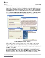
www.ti.com
Schematics and Bill of Materials
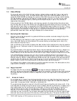
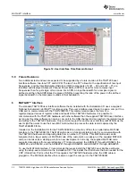
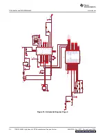
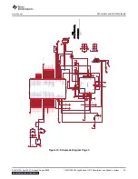
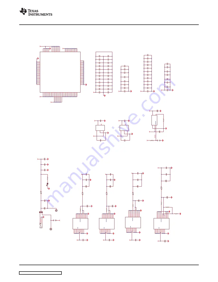
Figure 13. Schematic Diagram Page 1
SLAU212A – April 2007 – Revised August 2008
TSW1200EVM: High-Speed LVDS Deserializer and Analysis System
23


