background image

CH1_D4

CH1_D5

CH1_D6

CH1_D7

CH1_D8

CH1_D9

CH1_D10

CH1_D1

1

CH1_D0

CH1_D1

CH1_D2

CH1_D3

CH1_D12

CH1_D13

CH3_D6

CH3_D7

CH3_D8

CH3_D9

CH3_D10

CH3_D1

1

CH3_D12

CH3_D13

CH3_D1

CH3_D2

CH3_D3

CH3_D4

CH3_D5

CH3_D14

CH3_D15

CH4_D6

CH4_D7

CH4_D8

CH4_D9

CH4_D10

CH4_D1

1

CH4_D12

CH4_D13

CH4_D1

CH4_D2

CH4_D3

CH4_D4

CH4_D5

CH2_D6

CH2_D7

CH2_D8

CH2_D9

CH2_D10

CH2_D1

1

CH2_D12

CH2_D13

CH2_D0

CH2_D1

CH2_D2

CH2_D3

CH2_D4

CH2_D5

CH1-D0

CH1-D1

CH1-D2

CH1-D3

CH1-D4

CH1-D5

CH1-D6

CH1-D7

CH1-D8

CH1-D9

CH1-D10

CH1-D1

1

CH1-D12

CH1-D13

CH2-D0

CH2-D1

CH2-D2

CH2-D3

CH2-D4

CH2-D5

CH2-D6

CH2-D7

CH2-D9

CH2-D1

1

CH2-D12

CH2-D13

CH2-D14

CH2-D15

CH4-D1

CH1_CLKOUT

CH1-CLKOUT

CH3_CLKOUT

CH2_CLKOUT

CH4_CLKOUT

CH2-D10

CH2-D8

CH4-D2

CH4-D3

CH4-D4

CH4-D5

CH4-D6

CH4-D7

CH4-D8

CH4-D9

CH4-D10

CH4-D1

1

CH4-D12

CH4-D13

CH3-D1

CH3-D2

CH3-D3

CH3-D4

CH3-D5

CH3-D6

CH3-D7

CH3-D8

CH3-D9

CH3-D10

CH3-D1

1

CH3-D12

CH3-D13

CH3-D14

CH3-D15

CH3_D0

CH3-D0

CH4-D0

CH4_D0

CH2_D14

CH2_D15

CH2-CLKOUT

CH4-CLKOUT

CH3-CLKOUT

CH5_CLKOUT

CH5_D0

CH5_D1

CH5_D2

CH5_D3

CH5_D4

CH5_D5

CH5_D6

CH5_D7

CH5_D8

CH5_D9

CH5_D10

CH5_D1

1

CH5_D12

CH5_D13

CH6_D10

CH6_D1

1

CH6_CLKOUT

CH6_D12

CH6_D0

CH6_D13

CH6_D1

CH6_D2

CH6_D3

CH6_D4

CH6_D5

CH6_D6

CH6_D7

CH6_D8

CH6_D9

CH7_D10

CH7_D1

1

CH7_CLKOUT

CH7_D12

CH7_D0

CH7_D13

CH7_D1

CH7_D2

CH7_D3

CH7_D4

CH7_D5

CH7_D6

CH7_D7

CH7_D8

CH7_D9

CH8_D10

CH8_D1

1

CH8_CLKOUT

CH8_D12

CH8_D0

CH8_D13

CH8_D1

CH8_D2

CH8_D3

CH8_D4

CH8_D5

CH8_D6

CH8_D7

CH8_D8

CH8_D9

CH5-CLKOUT

SH3

CH5-D0

SH3

CH5-D1

SH3

CH5-D2

SH3

CH5-D3

SH3

CH5-D4

SH3

CH5-D5

SH3

CH5-D6

SH3

CH5-D7

SH3

CH5-D9

SH3

CH5-D10

SH3

CH5-D1

1

SH3

CH5-D12

SH3

CH5-D13

SH3

CH5-D8

SH3

CH6-D1

SH3

CH6-D2

SH3

CH6-D3

SH3

CH6-CLKOUT

SH3

CH6-D4

SH3

CH6-D5

SH3

CH6-D6

SH3

CH6-D7

SH3

CH6-D9

SH3

CH6-D10

SH3

CH6-D1

1

SH3

CH6-D12

SH3

CH6-D13

SH3

CH6-D8

SH3

CH6-D0

SH3

CH7-D1

SH3

CH7-D2

SH3

CH7-D3

SH3

CH7-CLKOUT

SH3

CH7-D4

SH3

CH7-D5

SH3

CH7-D6

SH3

CH7-D7

SH3

CH7-D9

SH3

CH7-D10

SH3

CH7-D1

1

SH3

CH7-D12

SH3

CH7-D13

SH3

CH7-D8

SH3

CH7-D0

SH3

CH8-D1

SH2

CH8-D2

SH2

CH8-D3

SH2

CH8-CLKOUT

SH2

CH8-D4

SH2

CH8-D5

SH2

CH8-D6

SH2

CH8-D7

SH2

CH8-D9

SH2

CH8-D10

SH2

CH8-D1

1

SH2

CH8-D12

SH2

CH8-D13

SH2

CH8-D8

SH2

CH8-D0

SH2

RN16

22ohm

RN16

22ohm

1

16

2

15

3

14

4

13

5

12

6

1

1

7

10

8

9

RN8

22ohm

RN8

22ohm

1

16

2

15

3

14

4

13

5

12

6

1

1

7

10

8

9

FD2

SMT

FIDUCIAL

FD2

SMT

FIDUCIAL

J20

HDR16X2MALE.100CTR

<TI_SILKTEXT>

J20

HDR16X2MALE.100CTR

<TI_SILKTEXT>

1

2

4

6

8

10

12

14

16

18

20

22

24

26

28

30

32

3

5

7

9

1

1

13

15

17

19

21

23

25

27

29

31

RN4

22ohm

RN4

22ohm

1

16

2

15

3

14

4

13

5

12

6

1

1

7

10

8

9

R61

22

R61

22

RN15

22ohm

RN15

22ohm

1

16

2

15

3

14

4

13

5

12

6

1

1

7

10

8

9

R63

22

R63

22

R60

22

R60

22

J5

HEADERMALE20x2POS.100VER

T

DA

T

A_OUT

J5

HEADERMALE20x2POS.100VER

T

DA

T

A_OUT

1

2

4

6

8

10

12

14

16

18

20

22

24

26

28

30

32

3

5

7

9

1

1

13

15

17

19

21

23

25

27

29

31

33

34

35

36

37

38

39

40

RN6

22ohm

RN6

22ohm

1

16

2

15

3

14

4

13

5

12

6

1

1

7

10

8

9

J18

HDR16X2MALE.100CTR

<TI_SILKTEXT>

J18

HDR16X2MALE.100CTR

<TI_SILKTEXT>

1

2

4

6

8

10

12

14

16

18

20

22

24

26

28

30

32

3

5

7

9

1

1

13

15

17

19

21

23

25

27

29

31

J6

HEADERMALE20x2POS.100VER

T

DA

T

A_OUT

J6

HEADERMALE20x2POS.100VER

T

DA

T

A_OUT

1

2

4

6

8

10

12

14

16

18

20

22

24

26

28

30

32

3

5

7

9

1

1

13

15

17

19

21

23

25

27

29

31

33

34

35

36

37

38

39

40

RN14

22ohm

RN14

22ohm

1

16

2

15

3

14

4

13

5

12

6

1

1

7

10

8

9

RN5

22ohm

RN5

22ohm

1

16

2

15

3

14

4

13

5

12

6

1

1

7

10

8

9

RN10

22ohm

RN10

22ohm

1

16

2

15

3

14

4

13

5

12

6

1

1

7

10

8

9

R62

22

R62

22

RN13

22ohm

RN13

22ohm

1

16

2

15

3

14

4

13

5

12

6

1

1

7

10

8

9

RN2

22ohm

RN2

22ohm

1

16

2

15

3

14

4

13

5

12

6

1

1

7

10

8

9

R29

22

R29

22

J21

HDR16X2MALE.100CTR

<TI_SILKTEXT>

J21

HDR16X2MALE.100CTR

<TI_SILKTEXT>

1

2

4

6

8

10

12

14

16

18

20

22

24

26

28

30

32

3

5

7

9

1

1

13

15

17

19

21

23

25

27

29

31

FD1

SMT

FIDUCIAL

FD1

SMT

FIDUCIAL

RN1

1

22ohm

RN1

1

22ohm

1

16

2

15

3

14

4

13

5

12

6

1

1

7

10

8

9

FD3

SMT

FIDUCIAL

FD3

SMT

FIDUCIAL

R30

22

R30

22

RN3

22ohm

RN3

22ohm

1

16

2

15

3

14

4

13

5

12

6

1

1

7

10

8

9

J4

HEADERMALE20x2POS.100VER

T

DA

T

A_OUT

J4

HEADERMALE20x2POS.100VER

T

DA

T

A_OUT

1

2

4

6

8

10

12

14

16

18

20

22

24

26

28

30

32

3

5

7

9

1

1

13

15

17

19

21

23

25

27

29

31

33

34

35

36

37

38

39

40

RN12

22ohm

RN12

22ohm

1

16

2

15

3

14

4

13

5

12

6

1

1

7

10

8

9

J19

HDR16X2MALE.100CTR

<TI_SILKTEXT>

J19

HDR16X2MALE.100CTR

<TI_SILKTEXT>

1

2

4

6

8

10

12

14

16

18

20

22

24

26

28

30

32

3

5

7

9

1

1

13

15

17

19

21

23

25

27

29

31

R28

22

R28

22

RN9

22ohm

RN9

22ohm

1

16

2

15

3

14

4

13

5

12

6

1

1

7

10

8

9

U1-3

XC4VLX25-SF363-BGA

U1-3

XC4VLX25-SF363-BGA

IO_L1P_6

B6

IO_L1N_6

A6

IO_L2P_6

A5

IO_L2N_6

B5

IO_L3P_6

C6

IO_L3N_6

C5

IO_L4P_6

B4

IO_L4N_VREF_6

C4

IO_L5P_6

D5

IO_L5N_6

E5

IO_L6P_6

A3

IO_L6N_6

B3

IO_L7P_6

D4

IO_L7N_6

D3

IO_L8P_CC_LC_6

B2

IO_L8N_CC_LC_6

C1

IO_L9P_CC_LC_6

F3

IO_L9N_CC_LC_6

E3

IO_L10P_6

C3

IO_L10N_6

C2

IO_L1

1P_6

F5

IO_L1

1N_6

F4

IO_L12P_6

D2

IO_L12N_VREF_6

E2

IO_L13P_6

G5

IO_L13N_6

G4

IO_L14P_6

E1

IO_L14N_6

F1

IO_L15P_6

H5

IO_L15N_6

H4

IO_L16P_6

F2

IO_L16N_6

G2

IO_L17P_6

J4

IO_L17N_6

J3

IO_L18P_6

H1

IO_L18N_6

G1

IO_L19P_6

J6

IO_L19N_6

J5

IO_L20P_6

H3

IO_L20N_VREF_6

H2

IO_L21P_6

K5

IO_L21N_6

K4

IO_L22P_6

K1

IO_L22N_6

J2

IO_L23P_VRN_6

L5

IO_L23N_VRP_6

L4

IO_L24P_CC_LC_6

K3

IO_L24N_CC_LC_6

K2

IO_L25P_CC_LC_6

M4

IO_L25N_CC_LC_6

M3

IO_L26P_6

M1

IO_L26N_6

L1

IO_L27P_6

M6

IO_L27N_6

M5

IO_L28P_6

M2

IO_L28N_VREF_6

L2

IO_L29P_6

N5

IO_L29N_6

N4

IO_L30P_6

N3

IO_L30N_6

N2

IO_L31P_6

P5

IO_L31N_6

P4

IO_L32P_6

P2

IO_L32N_6

P1

R27

22

R27

22

J3

HEADERMALE20x2POS.100VER

T

DA

T

A_OUT

J3

HEADERMALE20x2POS.100VER

T

DA

T

A_OUT

1

2

4

6

8

10

12

14

16

18

20

22

24

26

28

30

32

3

5

7

9

1

1

13

15

17

19

21

23

25

27

29

31

33

34

35

36

37

38

39

40

RN17

22ohm

RN17

22ohm

1

16

2

15

3

14

4

13

5

12

6

1

1

7

10

8

9

RN7

22ohm

RN7

22ohm

1

16

2

15

3

14

4

13

5

12

6

1

1

7

10

8

9

www.ti.com

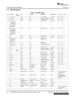
Schematics and Bill of Materials

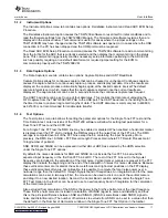
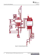
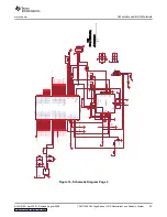
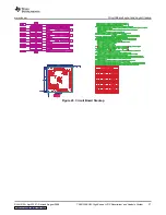
Figure 17. Schematic Diagram Page 5

SLAU212A – April 2007 – Revised August 2008

TSW1200EVM: High-Speed LVDS Deserializer and Analysis System

27

Submit Documentation Feedback

Summary of Contents for TSW1200EVM

Page 1: ...1200 User Interface Installation 13 8 Hardware Device Manager 14 9 Found New Hardware Windows 15 10 User Interface Initial Setup Screen 16 11 User Interface Single FFT format 20 12 User Interface Time...

Page 2: ...EW is a trademark of National Instruments Corporation MATLAB is a trademark of The MathWorks Inc Xilinx is a trademark of Xilinx Inc TSW1200EVM High Speed LVDS Deserializer and Analysis System 2 SLAU2...

Page 3: ...DS line one bit at a time at a higher data rate than the sample rate of the ADC The firmware in the FPGA on the TSW1200 is designed to accommodate both parallel DDR formats and serial LVDS formats alt...

Page 4: ...e ended CMOS output The TSW1200 FPGA has enough FIFO buffer to capture as much as a 65536 sample record length from the continuous sample data stream coming from the LVDS ADC interface The TSW1200 FPG...

Page 5: ...N TI recommends that the black banana jack J14 be connected to a bench ground even if the 6 V external power brick is connected to J7 Intermittent loss of the USB connection can sometimes be observed...

Page 6: ...FPGA Bit file CFG1 jumper J10 set to LO and jumper J11 set to HI is defined for use with ADC EVMs that employ a parallel LVDS DDR dual data rate format Bit file CFG2 is defined for use with ADC EVMs t...

Page 7: ...one JTAG device connected to the TDI of the next JTAG device The normal setting of the JTAG jumpers is to connect the TDI of the JTAG connector to the TDI pin of the FPGA EEPROM through jumper J12 pi...

Page 8: ...derived from the onboard oscillator LED D2 labeled DCM on the TSW1200 silkscreen which is an abbreviation for the digital clock manager block of logic in the FPGA flashes when an LVDS clock from the...

Page 9: ...amtec connector Fourteen LVDS data pairs plus two LVDS clock pairs have a defined position in the connector pinout that is common between the TSW1200EVM and many TI ADC EVMs For the parallel LVDS DDR...

Page 10: ...he operational mode of the ADC under evaluation There SPI signals are by default not connected on the ADC EVM until a 0 resistor is installed on the EVM to enable control of the SPI port from the TSW1...

Page 11: ...ure depth for an FFT on a million continuous data samples or more For this the output header posts are available so that a logic analyzer can be used to capture ADC data in real time The pinout of the...

Page 12: ...1200 Installation CD and are installed during the installation process The USB is accessed as a virtual communication port VCP and shows up in the Hardware Device Manager as TSW1200 under COM ports an...

Page 13: ...200 User Interface Installation If the TSW1200 user interface software is being installed on a machine that has an older version TI recommends that you first remove the old TSW1200 installation using...

Page 14: ...onnected the TSW1200EVM to the PC the TSW1200 can be located in the Hardware Device Manager as shown in Figure 8 The TSW1200 appears as TSW1200 as a COM port Each time the USB cable is connected it is...

Page 15: ...iguration for the PC If the Found New Hardware Wizard does appear again when the USB cable is reconnected follow the same responses to the dialog boxes as when the TSW1200 was first installed Figure 9...

Page 16: ...chosen from the test pulldown menu Figure 10 User Interface Initial Setup Screen The toolbar contains options and settings that are independent of the device selected for test or the test to be perfor...

Page 17: ...st Later revisions of the TSW1200 software will allow for setting test parameters for a Dual Tone FFT test and the ACPR test For a Single Tone FFT test the RMS line may be enabled or disabled When ena...

Page 18: ...nce statistics Time Domain displays the raw captured data in the format of a logic analyzer display and output level over time In the Window Display drop down menu the user chooses a windowing functio...

Page 19: ...marker to any place in the power spectrum such as a noise spur that is not already marked as a harmonic By default this additional marker initially goes to the highest spur that is not identified as...

Page 20: ...d third fourth and fifth harmonics of the input frequency and the user selectable marker are displayed in either dBFS or dBc Test setup Input parameters relevant to the test are repeated particularly...

Page 21: ...n results window In the upper half of the window the arithmetic value of the sample is represented on the vertical scale In the lower half of the window the individual bits of the data are displayed a...

Page 22: ...e can open a com port to the USB channel and can perform the register reads and writes to the TSW1200 hardware One common request for another user interface is MATLAB as the user might then want to us...

Page 23: ...1 2 C17 1uF C17 1uF 1 2 R109 300 R109 300 C44 01uF C44 01uF 1 2 C43 1uF C43 1uF 1 2 R58 24 3K R58 24 3K C349 10uF 10 16V C349 10uF 10 16V 1 2 C53 10uF 16V 10 LOW ESR C53 10uF 16V 10 LOW ESR C49 1uF C4...

Page 24: ...SDA 10 GND8 8 P3 3 30 P3 1 31 P3 0 32 GND28 28 X2 26 RI CP 16 DCD 15 VCC25 25 U1 4 XC4VLX25 SF363 BGA U1 4 XC4VLX25 SF363 BGA IO_L20P_7 R19 IO_L20N_VREF_7 R20 IO_L21P_7 R15 IO_L21N_7 R16 IO_L23P_VRN_7...

Page 25: ...F C79 10uF J10 HEADER 3 J10 HEADER 3 1 2 3 J2 J2 2 4 6 8 10 12 14 1 3 5 7 9 11 13 C86 1uF C86 1uF 1 2 R3 0 ohm R3 0 ohm C83 3 3uF C83 3 3uF R52 4 7K R52 4 7K R2 0 ohm R2 0 ohm R33 1K R33 1K Q3 DTC114E...

Page 26: ...6 IO_L4P_5 B17 IO_L4N_VREF_5 C17 IO_L5P_5 D16 IO_L5N_5 E16 IO_L6P_5 A18 IO_L6N_5 B18 IO_L7P_5 D17 IO_L7N_5 D18 IO_L8P_CC_LC_5 B19 IO_L8N_CC_LC_5 C20 IO_L9P_CC_LC_5 F18 IO_L9N_CC_LC_5 E18 IO_L10P_5 C18...

Page 27: ...10 8 9 J18 HDR 16X2 MALE 100CTR TI_SILKTEXT J18 HDR 16X2 MALE 100CTR TI_SILKTEXT 1 2 4 6 8 10 12 14 16 18 20 22 24 26 28 30 32 3 5 7 9 11 13 15 17 19 21 23 25 27 29 31 J6 HEADER MALE 20x2 POS 100 VERT...

Page 28: ...onic 10 10V 2 C77 C78 22 pF 603 GRM1885C2A220JA01D Murata 5 100V 2 C81 C85 0 1 F 603 ECJ 1VB1H104K Panasonic 10 50V 2 C82 C84 2 2 F 603 ECJ 1VB1A225K Panasonic 10 10V 1 C83 3 3 F TANT_B TAJB335K016R A...

Page 29: ...o 1 1 10W 8 R27 R30 22 603 RC0603FR 0722RL Yageo 1 1 10W R60 R63 6 R33 R34 R37 R 1K 603 ERJ 3EKF1001V Panasonic 1 1 10W 38 R46 R47 2 R35 R36 100 603 ERJ 3EKF1000V Panasonic 1 1 10W 1 R45 100K 603 ERJ...

Page 30: ...I Provide pad 1 U14 PTH03000W SMD_PWRMOD_EUT5 PTH03000WAS TI TI Provide 1 U15 TPS73225 SOT23 DBV5 TPS73225DBVT TI TI Provide 1 Y1 12MHz w 18pF smd_xtal_AMB3B ABM3B 12 000MHZ 10 1 Abracon U T 4 Screw 4...

Page 31: ...m Circuit Board Layout and Layer Stackup Figure 19 TSW1200C Layout Layer Two SLAU212A April 2007 Revised August 2008 TSW1200EVM High Speed LVDS Deserializer and Analysis System 31 Submit Documentation...

Page 32: ...ard Layout and Layer Stackup www ti com Figure 20 TSW1200C Layout Power Plane 32 TSW1200EVM High Speed LVDS Deserializer and Analysis System SLAU212A April 2007 Revised August 2008 Submit Documentatio...

Page 33: ...Circuit Board Layout and Layer Stackup Figure 21 TSW1200C Layout Ground Plane SLAU212A April 2007 Revised August 2008 TSW1200EVM High Speed LVDS Deserializer and Analysis System 33 Submit Documentatio...

Page 34: ...Board Layout and Layer Stackup www ti com Figure 22 TSW1200C Layout Layer 5 34 TSW1200EVM High Speed LVDS Deserializer and Analysis System SLAU212A April 2007 Revised August 2008 Submit Documentation...

Page 35: ...i com Circuit Board Layout and Layer Stackup Figure 23 TSW1200C Layer 6 SLAU212A April 2007 Revised August 2008 TSW1200EVM High Speed LVDS Deserializer and Analysis System 35 Submit Documentation Feed...

Page 36: ...Board Layout and Layer Stackup www ti com Figure 24 TSW1200C Bottom Layer 36 TSW1200EVM High Speed LVDS Deserializer and Analysis System SLAU212A April 2007 Revised August 2008 Submit Documentation F...

Page 37: ...com Circuit Board Layout and Layer Stackup Figure 25 Circuit Board Stackup SLAU212A April 2007 Revised August 2008 TSW1200EVM High Speed LVDS Deserializer and Analysis System 37 Submit Documentation F...

Page 38: ...uct This notice contains important safety information about temperatures and voltages For additional information on TI s environmental and or safety programs please contact the TI application engineer...

Page 39: ...siness practice TI is not responsible or liable for any such statements TI products are not authorized for use in safety critical applications such as life support where a failure of the TI product wo...

Page 40: ...Mouser Electronics Authorized Distributor Click to View Pricing Inventory Delivery Lifecycle Information Texas Instruments TSW1200EVM...

Reviews: