

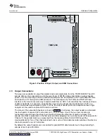


TSW1200
6 V Input
Ground
HEADER POSTS
HEADER POSTS
HEADER POSTS
HEADER POSTS
CLK
GND
GND
CLK
J6 ch 4
J21 ch 8
JT
AG
L
VDS
L
VDS
USB
HEADERPOSTS
HEADERPOSTS
HEADERPOSTS
HEADERPOSTS
CLK
GND
CLK
GND
J18 ch 5
6 V I/O
J3 ch 1
3.5
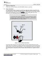
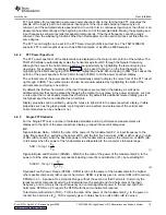
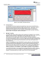
Output Connections
www.ti.com
Hardware Configuration
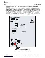
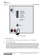
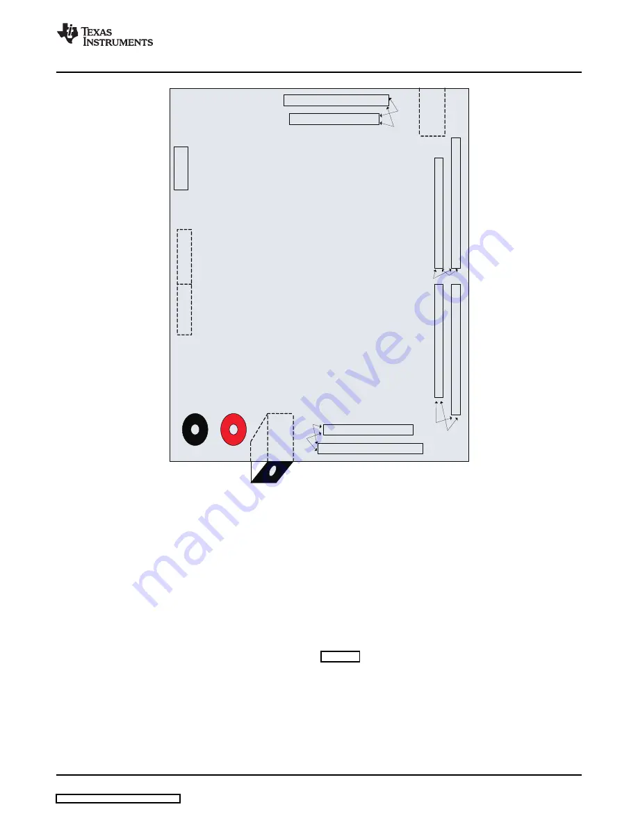
Figure 5. Position of Input, Output, and USB Connections
Two ways are available to output the parallel clock and sample data from the TSW1200EVM. The ADC
sample data can be presented as a continuous stream of CMOS single-ended data on output header
posts, or a set record length of ADC parallel data samples can be captured in the TSW1200EVM FIFOs
and output to a PC through the USB serial port. The data capture by the FIFOs and TSW1200 user
interface is the most convenient way to capture data from an ADC, but sometimes the continuous stream
of data is desirable. For example, an application may require a larger capture depth for an FFT on a
million continuous data samples or more. For this, the output header posts are available so that a logic
analyzer can be used to capture ADC data in real time.
The pinout of the output data headers is shown in
. In all cases, the output header is a standard
two-row header of square 0.025-inch posts on 0.1-inch centers. One of the two rows of posts are
connected to ground down the whole row of posts, whereas the other row of posts are signal. The
sample-rate clock is presented on the first post, and after skipping one no-connect post (or three posts for
Channel 1) the parallel data bus is presented from the least-significant bit (bit D0) through the
most-significant bit. Two of the channels allow for as much as 16-bit data resolution whereas the other six
channels provide for up to 14-bit data.
By default, the output headers are not enabled for parallel DDR data formats due to the potential high
sample rates of up to 500 MHz.
SLAU212A – April 2007 – Revised August 2008
TSW1200EVM: High-Speed LVDS Deserializer and Analysis System
11


