


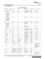


PROG_B
TDI_0
M0
M2
M1
DO
NE
CE
TDO_0
TDO
TCK
TMS
TDI
HSW
AP_EN
CC
LK
BUSY
PROMRESET
+3.3V
+3.3V
+3.3V
+3.3V
+3.3V
+3.3V
+1.8V
+3.3V
+1.8V
+3.3V
+3.3V
+3.3V
+3.3V
+3.3V
D6
D7
D5
D2
D4
D3
D0
D1
D0
D1
D2
D3
D4
D5
D6
D7
CH7-CLKOUT
SH5
CH7-D0
SH5
CH6-D1
SH5
CH6-D2
SH5
CH6-D3
SH5
CH6-D4
SH5
CH6-D5
SH5
CH6-D0
SH5
CH5-D3
SH5
CH5-D4
SH5
CH5-D5
SH5
CH5-D6
SH5
CH5-D7
SH5
CH5-D9
SH5
CH5-D10
SH5
CH5-D1
1
SH5
CH5-D12
SH5
CH5-D13
SH5
CH5-D8
SH5
CH6-CLKOUT
SH5
CH6-D7
SH5
CH6-D9
SH5
CH6-D10
SH5
CH6-D1
1
SH5
CH6-D6
SH5
CH6-D8
SH5
CH6-D12
SH5
CH6-D13
SH5
CH5-CLKOUT
SH5
CH5-D0
SH5
CH5-D2
SH5
CH5-D1
SH5
CH7-D3
SH5
CH7-D1
SH5
CH7-D2
SH5
CH7-D4
SH5
CH7-D12
SH5
CH7-D13
SH5
CH7-D5
SH5
CH7-D6
SH5
CH7-D7
SH5
CH7-D8
SH5
CH7-D9
SH5
CH7-D1
1
SH5
CH7-D10
SH5
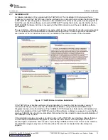
JTAG
1.DEFAULTSETUPFORJ1ANDJ12
SHORT1AND3;SHORT2AND4
2.PROMCONFIGURATION
M0=M1=1
SETUPFORMASTERSELECTMAPOPERATION
M2=0
NOTES:
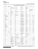
D7
GREEN
D7
GREEN
R4
10K
R4
10K
R35
100
R35
100
R1
0ohm
R1
0ohm
U2
XCF32PFSG48
U2
XCF32PFSG48
D3
D5
NC1
A4
D7
A6
VCCO
B2
CE
B4
CL
KO
UT
C2
D4
C5
CE
O
D2
GND
A1
GND
A2
OE/RESET
A3
D6
A5
VCCINT
B1
CLK
B3
D5
B5
GND
B6
BUS
Y
C1
NC2
C3
NC3
C4
VC
CO
C6
CF
D1
NC4
D3
NC5
D4
VC
CO
D6
TMS
E2
VCCINT
E1
NC7
E4
NC6
E3
D2
E5
TDO
E6
GND
F1
NC8
F2
NC10
F4
NC9
F3
GND
F5
GND
F6
TD
I
G1
NC
11
G2
REV_SEL0
G3
REV_SEL1
G4
VC
CO
G5
VC
CIN
T
G6
GND
H1
VC
CJ
H2
TC
K
H3
EN_
EX
T_
SE
L
H4
D1
H5
D0
H6
C4
.1uF
C4
.1uF
1
2
R55
ZERO
R55
ZERO
R32
0ohm
R32
0ohm
C1
10uF
C1
10uF
C6
.1uF
C6
.1uF
1
2
RN1
4.7K
RN1
4.7K
1
8
2
7
3
6
4
5
C5
.01uF
C5
.01uF
1
2
R7
330
R7
330
C3
.01uF
C3
.01uF
1
2
R54
49.9
R54
49.9
R6
4.7K
R6
4.7K
J1J1
1
2
4
3
C2
.1uF
C2
.1uF
1
2
SW2
RESET
SW2
RESET
1
2
SW3
PROGRAM
SW3
PROGRAM
1
2
C80
.1uF
C80
.1uF
1
2
R31
0ohm
R31
0ohm
R53
49.9
R53
49.9
U10
L
V7745DEV
-200MHz
U10
L
V7745DEV
-200MHz
OE
1
NC
2
GND
3
OUT
4
OUT
5
VCC
6
J12J12
1
2
4
3
R36
100
R36
100
C87
.1uF
C87
.1uF
1
2
C79
10uF
C79
10uF
J10
HEADER3
J10
HEADER3
1
2
3
J2J2
2
4
6
8
10
12
14
1
3
5
7
9
1
1
13
C86
.1uF
C86
.1uF
1
2
R3
0ohm
R3
0ohm
+
C83
3.3uF
+
C83
3.3uF
R52
4.7K
R52
4.7K
R2
0ohm
R2
0ohm
R33
1K
R33
1K
Q3
DTC1
14EET1
Q3
DTC1
14EET1
J1
1
HEADER3
J1
1
HEADER3
1
2
3
R34
1K
R34
1K
U1-1
XC4VLX25-SF363-BGA
U1-1
XC4VLX25-SF363-BGA
HSW
APEN_0
E13
CCLK_0
E1
1
D_IN_0
E9
CS_B_0
E8
INIT_B_0
E12
TDN_0
E10
RDWR_B_0
F9
TDP_0
F10
DONE_0
F1
1
PROG_B_0
F12
TDI_0
R9
TDO_0
R10
M2_0
R1
1
M0_0
R12
TMS_0
T8
TCK_0
T9
PWRDWN_B_0
T10
DOUT_BUSY_0
T1
1
M1_0
T12
VBA
TT_0
T13
IO_L1P_D31_LC_1
F15
IO_L1N_D30_LC_1
E15
IO_L2P_D29_LC_1
E6
IO_L2N_D28_LC_1
F6
IO_L3P_D27_LC_1
D15
IO_L3N_D26_LC_1
E14
IO_L4P_D25_LC_1
E7
IO_L4N_D24_VREF_LC_1
D6
IO_L5P_D23_LC_1
D13
IO_L5N_D22_LC_1
C13
IO_L6P_D21_LC_1
C8
IO_L6N_D20_LC_1
D8
IO_L7P_D19_LC_1
D12
IO_L7N_D18_LC_1
C12
IO_L8P_D17_CC_LC_1
C9
IO_L8N_D16_CC_LC_1
D9
IO_L1P_GC_CC_LC_3
B12
IO_L1N_GC_CC_LC_3
A1
1
IO_L2P_GC_VRN_LC_3
A10
IO_L2N_GC_VRP_LC_3
B9
IO_L3P_GC_LC_3
C1
1
IO_L3N_GC_LC_3
B1
1
IO_L4P_GC_LC_3
B10
IO_L4N_GC_VREF_LC_3
C10
IO_L5P_GC_LC_3
B13
IO_L5N_GC_LC_3
A13
IO_L6P_GC_LC_3
A8
IO_L6N_GC_LC_3
B8
IO_L7P_GC_LC_3
B14
IO_L7N_GC_LC_
A14
IO_L8P_GC_LC_3
A7
IO_L8N_GC_LC_3
B7
IO_L1P_D15_CC_LC_2
V16
IO_L1N_D14_CC_LC_2
V15
IO_L2P_D13_LC_2
V6
IO_L2N_D12_LC_2
V5
IO_L3P_D1
1_LC_2
T14
IO_L3N_D10_LC_2
U13
IO_L4P_D9_LC_2
U8
IO_L4N_D8_VREF_LC_2
T7
IO_L5P_D7_LC_2
V13
IO_L5N_D6_LC_1
1
V12
IO_L6P_D5_LC_2
V9
IO_L6N_D4_LC_2
V8
IO_L7P_D3_LC_2
U12
IO_L7N_D2_LC_2
V1
1
IO_L8P_D1_LC_2
V10
IO_L8N_D0_LC_2
U9
IO_L1P_GC_LC_4
W13
IO_L1N_GC_LC_4
W12
IO_L2P_GC_LC_4
Y5
IO_L2N_GC_LC_4
W5
IO_L3P_GC_LC_4
Y12
IO_L3N_GC_LC_4
Y1
1
IO_L4P_GC_LC_4
Y6
IO_L4N_GC_VREF_LC_4
W6
IO_L5P_GC_LC_4
W1
1
IO_L5N_GC_LC_4
W10
IO_L6P_GC_LC_4
Y7
IO_L6N_GC_LC_4
W7
IO_L7P_GC_VRN_LC_4
Y10
IO_L7N_GC_VRP_LC_4
Y9
IO_L8P_GC_CC_LC_4
W9
IO_L8N_GC_CC_LC_4
W8
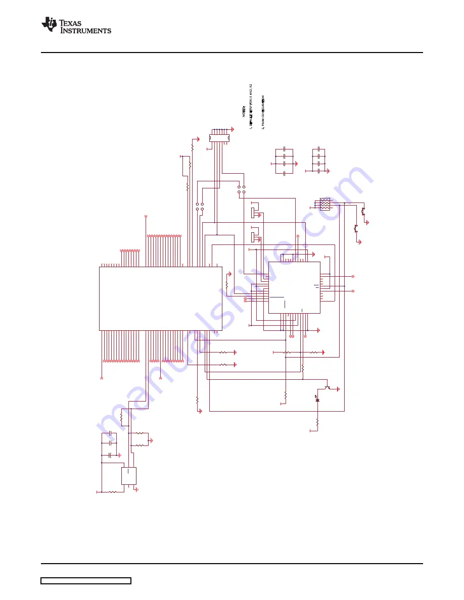
www.ti.com
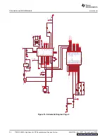
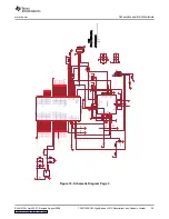
Schematics and Bill of Materials
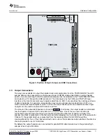
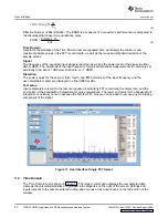
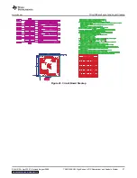
Figure 15. Schematic Diagram Page 3
SLAU212A – April 2007 – Revised August 2008
TSW1200EVM: High-Speed LVDS Deserializer and Analysis System
25


