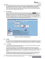
background image

1

Introduction

2

Functionality

www.ti.com

Introduction

The Texas Instruments TSW1200 High-Speed LVDS Deserializer and Analysis System provides a
comprehensive set of hardware and user interface software to effectively evaluate the performance of a
wide range of Texas Instruments (TI) high-speed, analog- to-digital converters (ADC), particularly those
high-speed ADCs that employ an low-voltage differential signal (LVDS) format for the data converter’s
output data. With a high-quality, low-jitter clock and a high-quality input frequency provided to the
evaluation module, the TSW1200 system can be used to demonstrate data sheet performance
specifications.

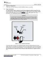
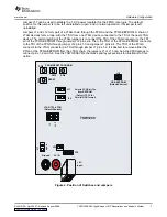
The TSW1200 hardware has a high-speed connector that plugs into an evaluation module (EVM) for the
ADC. Firmware for an FPGA on the TSW1200EVM has an interface to various LVDS data formats and
FIFO memory sufficient to capture as much as 64K samples of data. A USB connection transfers the
captured data to a personal computer for post-processing. The user Interface software controls the
TSW1200 hardware and displays the FFT and important statistics related to the performance of the ADC.

Many TI high-speed ADCs have LVDS outputs for the digitized data. These ADCs are generally available
on an EVM that connects directly to the TSW1200EVM. The common connector between the ADC EVM
and the TSW1200EVM is a Samtec high-speed connector suitable for differential pairs of pins separated
by ground. A common pinout for the connector across a family of EVMs has been established. At present,
the interface between the ADC EVM and the TSW1200EVM has defined connections for 14 pairs of LVDS
plus two clock lines. The connector pinout has an additional 14 LVDS pairs for future product support. In
most cases, if a TI ADC supports LVDS outputs, then the TSW1200 system can be used to capture data
from the ADC. If the ADC supports a CMOS single-ended format, then the TSW1100 system is intended
to interface to it.

The data format for the LVDS data bus can be in one of many formats, all supported by the TSW1200.
For single-channel, high-speed ADCs, the data format is commonly parallel dual-data rate with one clock
line. Dual-data rate means that both the rising and falling edges of the clock strobe data into the
TSW1200. For multichannel ADCs, the data is commonly presented in a serialized format, where
individual bits of the output data are presented on an LVDS line one bit at a time, at a higher data rate
than the sample rate of the ADC.

The firmware in the FPGA on the TSW1200 is designed to accommodate both parallel DDR formats and
serial LVDS formats, although not at the same time. The EEPROM on the TSW1200EVM is large enough
to hold two distinct program files for the FPGA. One program bit file supports the parallel DDR format and
the other bit file supports serial LVDS formats. The TSW1200 can be set to support the desired data
format by simply setting two jumpers and pressing the PROGRAM button.

The parallel DDR FPGA program supports several types of data formats. One common format presents
odd-numbered data bits on the bus on one clock edge and even-numbered data bits on the bus on the
other clock edge. This format is commonly used for ADCs with sampling rates up to 250 MHz. For this
bit-wise DDR format, the parallel data bus uses half as many LVDS pairs as there are bits in the sample.
For example, a 16-bit ADC uses eight LVDS pairs for data plus an LVDS clock pair for bit-wise DDR. For
higher sample rates up to 500 MHz, a sample-wise DDR format is often used. For sample-wise DDR, the
data bus width has as many LVDS pairs as the bit resolution of the ADC. On one clock edge, a data
sample from the ADC is registered; on the next clock edge, the next data sample from the ADC is
registered.

The serial FPGA program also supports several data formats. For one-wire serial formats, the data is
serialized onto a single LVDS pair at a rate that is 12 times the sample rate for an ADC with a 12-bit
resolution. A one-wire serialization format also is used for 14-bit and 16-bit data at data rates 14 or 16
times the sample rate, respectively. For serial data formats, a DDR LVDS bit clock is used to strobe the
serial data bits and to deserialize the data. An additional clock pair provided at the sample rate of the ADC
identifies the sample-word boundaries in the serial data. For multichannel ADCs, a single-bit clock and a
single sample-rate clock (frame clock) is used for all of the LVDS data channels. The other common serial
data format is two-wire serialization. Two-wire serialization is similar to one-wire serialization except that a
data channel uses two LVDS pairs to carry the serialized data at a rate that is half of what it is for one-wire
serialization. Two-wire serialization commonly is used for sample rates up to 125 MHz, whereas one-wire
serialization generally is used for sample rates up to 65 MHz.

SLAU212A – April 2007 – Revised August 2008

TSW1200EVM: High-Speed LVDS Deserializer and Analysis System

3

Submit Documentation Feedback

Summary of Contents for TSW1200EVM

Page 1: ...1200 User Interface Installation 13 8 Hardware Device Manager 14 9 Found New Hardware Windows 15 10 User Interface Initial Setup Screen 16 11 User Interface Single FFT format 20 12 User Interface Time...

Page 2: ...EW is a trademark of National Instruments Corporation MATLAB is a trademark of The MathWorks Inc Xilinx is a trademark of Xilinx Inc TSW1200EVM High Speed LVDS Deserializer and Analysis System 2 SLAU2...

Page 3: ...DS line one bit at a time at a higher data rate than the sample rate of the ADC The firmware in the FPGA on the TSW1200 is designed to accommodate both parallel DDR formats and serial LVDS formats alt...

Page 4: ...e ended CMOS output The TSW1200 FPGA has enough FIFO buffer to capture as much as a 65536 sample record length from the continuous sample data stream coming from the LVDS ADC interface The TSW1200 FPG...

Page 5: ...N TI recommends that the black banana jack J14 be connected to a bench ground even if the 6 V external power brick is connected to J7 Intermittent loss of the USB connection can sometimes be observed...

Page 6: ...FPGA Bit file CFG1 jumper J10 set to LO and jumper J11 set to HI is defined for use with ADC EVMs that employ a parallel LVDS DDR dual data rate format Bit file CFG2 is defined for use with ADC EVMs t...

Page 7: ...one JTAG device connected to the TDI of the next JTAG device The normal setting of the JTAG jumpers is to connect the TDI of the JTAG connector to the TDI pin of the FPGA EEPROM through jumper J12 pi...

Page 8: ...derived from the onboard oscillator LED D2 labeled DCM on the TSW1200 silkscreen which is an abbreviation for the digital clock manager block of logic in the FPGA flashes when an LVDS clock from the...

Page 9: ...amtec connector Fourteen LVDS data pairs plus two LVDS clock pairs have a defined position in the connector pinout that is common between the TSW1200EVM and many TI ADC EVMs For the parallel LVDS DDR...

Page 10: ...he operational mode of the ADC under evaluation There SPI signals are by default not connected on the ADC EVM until a 0 resistor is installed on the EVM to enable control of the SPI port from the TSW1...

Page 11: ...ure depth for an FFT on a million continuous data samples or more For this the output header posts are available so that a logic analyzer can be used to capture ADC data in real time The pinout of the...

Page 12: ...1200 Installation CD and are installed during the installation process The USB is accessed as a virtual communication port VCP and shows up in the Hardware Device Manager as TSW1200 under COM ports an...

Page 13: ...200 User Interface Installation If the TSW1200 user interface software is being installed on a machine that has an older version TI recommends that you first remove the old TSW1200 installation using...

Page 14: ...onnected the TSW1200EVM to the PC the TSW1200 can be located in the Hardware Device Manager as shown in Figure 8 The TSW1200 appears as TSW1200 as a COM port Each time the USB cable is connected it is...

Page 15: ...iguration for the PC If the Found New Hardware Wizard does appear again when the USB cable is reconnected follow the same responses to the dialog boxes as when the TSW1200 was first installed Figure 9...

Page 16: ...chosen from the test pulldown menu Figure 10 User Interface Initial Setup Screen The toolbar contains options and settings that are independent of the device selected for test or the test to be perfor...

Page 17: ...st Later revisions of the TSW1200 software will allow for setting test parameters for a Dual Tone FFT test and the ACPR test For a Single Tone FFT test the RMS line may be enabled or disabled When ena...

Page 18: ...nce statistics Time Domain displays the raw captured data in the format of a logic analyzer display and output level over time In the Window Display drop down menu the user chooses a windowing functio...

Page 19: ...marker to any place in the power spectrum such as a noise spur that is not already marked as a harmonic By default this additional marker initially goes to the highest spur that is not identified as...

Page 20: ...d third fourth and fifth harmonics of the input frequency and the user selectable marker are displayed in either dBFS or dBc Test setup Input parameters relevant to the test are repeated particularly...

Page 21: ...n results window In the upper half of the window the arithmetic value of the sample is represented on the vertical scale In the lower half of the window the individual bits of the data are displayed a...

Page 22: ...e can open a com port to the USB channel and can perform the register reads and writes to the TSW1200 hardware One common request for another user interface is MATLAB as the user might then want to us...

Page 23: ...1 2 C17 1uF C17 1uF 1 2 R109 300 R109 300 C44 01uF C44 01uF 1 2 C43 1uF C43 1uF 1 2 R58 24 3K R58 24 3K C349 10uF 10 16V C349 10uF 10 16V 1 2 C53 10uF 16V 10 LOW ESR C53 10uF 16V 10 LOW ESR C49 1uF C4...

Page 24: ...SDA 10 GND8 8 P3 3 30 P3 1 31 P3 0 32 GND28 28 X2 26 RI CP 16 DCD 15 VCC25 25 U1 4 XC4VLX25 SF363 BGA U1 4 XC4VLX25 SF363 BGA IO_L20P_7 R19 IO_L20N_VREF_7 R20 IO_L21P_7 R15 IO_L21N_7 R16 IO_L23P_VRN_7...

Page 25: ...F C79 10uF J10 HEADER 3 J10 HEADER 3 1 2 3 J2 J2 2 4 6 8 10 12 14 1 3 5 7 9 11 13 C86 1uF C86 1uF 1 2 R3 0 ohm R3 0 ohm C83 3 3uF C83 3 3uF R52 4 7K R52 4 7K R2 0 ohm R2 0 ohm R33 1K R33 1K Q3 DTC114E...

Page 26: ...6 IO_L4P_5 B17 IO_L4N_VREF_5 C17 IO_L5P_5 D16 IO_L5N_5 E16 IO_L6P_5 A18 IO_L6N_5 B18 IO_L7P_5 D17 IO_L7N_5 D18 IO_L8P_CC_LC_5 B19 IO_L8N_CC_LC_5 C20 IO_L9P_CC_LC_5 F18 IO_L9N_CC_LC_5 E18 IO_L10P_5 C18...

Page 27: ...10 8 9 J18 HDR 16X2 MALE 100CTR TI_SILKTEXT J18 HDR 16X2 MALE 100CTR TI_SILKTEXT 1 2 4 6 8 10 12 14 16 18 20 22 24 26 28 30 32 3 5 7 9 11 13 15 17 19 21 23 25 27 29 31 J6 HEADER MALE 20x2 POS 100 VERT...

Page 28: ...onic 10 10V 2 C77 C78 22 pF 603 GRM1885C2A220JA01D Murata 5 100V 2 C81 C85 0 1 F 603 ECJ 1VB1H104K Panasonic 10 50V 2 C82 C84 2 2 F 603 ECJ 1VB1A225K Panasonic 10 10V 1 C83 3 3 F TANT_B TAJB335K016R A...

Page 29: ...o 1 1 10W 8 R27 R30 22 603 RC0603FR 0722RL Yageo 1 1 10W R60 R63 6 R33 R34 R37 R 1K 603 ERJ 3EKF1001V Panasonic 1 1 10W 38 R46 R47 2 R35 R36 100 603 ERJ 3EKF1000V Panasonic 1 1 10W 1 R45 100K 603 ERJ...

Page 30: ...I Provide pad 1 U14 PTH03000W SMD_PWRMOD_EUT5 PTH03000WAS TI TI Provide 1 U15 TPS73225 SOT23 DBV5 TPS73225DBVT TI TI Provide 1 Y1 12MHz w 18pF smd_xtal_AMB3B ABM3B 12 000MHZ 10 1 Abracon U T 4 Screw 4...

Page 31: ...m Circuit Board Layout and Layer Stackup Figure 19 TSW1200C Layout Layer Two SLAU212A April 2007 Revised August 2008 TSW1200EVM High Speed LVDS Deserializer and Analysis System 31 Submit Documentation...

Page 32: ...ard Layout and Layer Stackup www ti com Figure 20 TSW1200C Layout Power Plane 32 TSW1200EVM High Speed LVDS Deserializer and Analysis System SLAU212A April 2007 Revised August 2008 Submit Documentatio...

Page 33: ...Circuit Board Layout and Layer Stackup Figure 21 TSW1200C Layout Ground Plane SLAU212A April 2007 Revised August 2008 TSW1200EVM High Speed LVDS Deserializer and Analysis System 33 Submit Documentatio...

Page 34: ...Board Layout and Layer Stackup www ti com Figure 22 TSW1200C Layout Layer 5 34 TSW1200EVM High Speed LVDS Deserializer and Analysis System SLAU212A April 2007 Revised August 2008 Submit Documentation...

Page 35: ...i com Circuit Board Layout and Layer Stackup Figure 23 TSW1200C Layer 6 SLAU212A April 2007 Revised August 2008 TSW1200EVM High Speed LVDS Deserializer and Analysis System 35 Submit Documentation Feed...

Page 36: ...Board Layout and Layer Stackup www ti com Figure 24 TSW1200C Bottom Layer 36 TSW1200EVM High Speed LVDS Deserializer and Analysis System SLAU212A April 2007 Revised August 2008 Submit Documentation F...

Page 37: ...com Circuit Board Layout and Layer Stackup Figure 25 Circuit Board Stackup SLAU212A April 2007 Revised August 2008 TSW1200EVM High Speed LVDS Deserializer and Analysis System 37 Submit Documentation F...

Page 38: ...uct This notice contains important safety information about temperatures and voltages For additional information on TI s environmental and or safety programs please contact the TI application engineer...

Page 39: ...siness practice TI is not responsible or liable for any such statements TI products are not authorized for use in safety critical applications such as life support where a failure of the TI product wo...

Page 40: ...Mouser Electronics Authorized Distributor Click to View Pricing Inventory Delivery Lifecycle Information Texas Instruments TSW1200EVM...

Reviews: