background image

TUSB522P EVM Configuration

www.ti.com

4

SLLU244 – August 2016

Submit Documentation Feedback

Copyright © 2016, Texas Instruments Incorporated

TUSB522P EVM

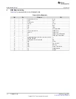
Table 1. Jumper / Switch Description and Settings

Jumper

Functionality and Configuration

J1

EQ1

1-2 = 1 (1K to VCC)

3-4 = R (20K to GND)

5-6 = 0 (1K to GND)

NC = F (No Connect)

J2

DE2

1-2 = 1 (1K to VCC)

3-4 = R (20K to GND)

5-6 = 0 (1K to GND)

NC = F (No Connect)

J3

DE1

1-2 = 1 (1K to VCC)

3-4 = R (20K to GND)

5-6 = 0 (1K to GND)

NC = F (No Connect)

J4

EQ2

1-2 = 1 (1K to VCC)

3-4 = R (20K to GND)

5-6 = 0 (1K to GND)

NC = F (No Connect)

J5

OS2

1-2 = 1 (1K to VCC)

3-4 = R (20K to GND)

5-6 = 0 (1K to GND)

NC = F (No Connect)

J6

NC2

1-2 = 1 (1K to VCC)

3-4 = R (20K to GND)

5-6 = 0 (1K to GND)

NC = F (No Connect)

J7

NC1

1-2 = 1 (1K to VCC)

3-4 = R (20K to GND)

5-6 = 0 (1K to GND)

NC = F (No Connect)

J8

OS1

1-2 = 1 (1K to VCC)

3-4 = R (20K to GND)

5-6 = 0 (1K to GND)

NC = F (No Connect)

J9/SW1

EN_RXD (Shutdown Mode)

1-2 = 1K to GND

NC = Internal Pull-up (Default)

SW1 = Push to Short EN to GND

J10

RSVD

1-2 = 1K to GND

NC = Internal Pull-up (Default)

J11

VCC 3.3V

1-2 = VCC_3.3V Provided from U2 (Default)

NC = Provide external 3.3 V on Pin 2

Summary of Contents for TUSB522P

Page 1: ... application Target applications include cell phones computers docking stations TVs and active cables Schematic and layout information is included at the end of this manual Contents 1 Introduction 2 2 TUSB522P EVM Configuration 3 2 1 Description of EVM Board 3 2 2 TUSB522P Configuration Pins 5 2 3 Monitoring the Device Current 5 3 PCB Construction 6 3 1 TUSB522P EVM Board Schematics 6 3 2 TUSB522P...

Page 2: ...1 0 supporting electrical idle condition and low frequency periodic signals LFPS for USB 3 1 power management modes The device offers programmable equalization that extends the interconnect distance between two devices Also the device supports low power modes when unplugged The device can also function in USB compliance mode to test the transmitter for compliance to voltage and timing specificatio...

Page 3: ...ms TUSB522P EVM board This user s manual 2 1 Description of EVM Board The TUSB522P EVM is designed to provide easy evaluation of the TUSB522P device It is also meant to serve as a reference design to show a practical example of how to use the device in a mass production system Figure 2 highlights the jumpers and switch installed on this EVM and Table 1 highlights their functionality and configurat...

Page 4: ... 0 1K to GND NC F No Connect J4 EQ2 1 2 1 1K to VCC 3 4 R 20K to GND 5 6 0 1K to GND NC F No Connect J5 OS2 1 2 1 1K to VCC 3 4 R 20K to GND 5 6 0 1K to GND NC F No Connect J6 NC2 1 2 1 1K to VCC 3 4 R 20K to GND 5 6 0 1K to GND NC F No Connect J7 NC1 1 2 1 1K to VCC 3 4 R 20K to GND 5 6 0 1K to GND NC F No Connect J8 OS1 1 2 1 1K to VCC 3 4 R 20K to GND 5 6 0 1K to GND NC F No Connect J9 SW1 EN_R...

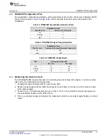
Page 5: ...evel Transition Bit Output Differential Voltage mV Low 900 High 1200 Table 4 TUSB522P De Emphasis DEx De Emphasis Ratio dB OS Low OS High Low 0 2 6 Floating 3 5 5 9 High 6 2 8 3 2 3 Monitoring the Device Current The TUSB522P EVM includes the option of monitoring the current draw of the device In order to enable this feature the following steps must be taken 1 Un install the shunt located at JMP11 ...

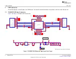
Page 6: ...f C7 1uf U1 TUSB522PRGE VCC 1 EQ1 2 DE2 3 OS2 4 EN_RXD 5 NC 6 NC 7 RX1N 8 RX1P 9 GND 10 TX2N 11 TX2P 12 VCC 13 RSV 14 OS1 15 DE1 16 EQ2 17 NC 18 RX2P 19 RX2N 20 GND 21 TX1P 22 TX1N 23 NC 24 PAD 25 P1 USB3 0 Type B Receptacle VBUS 1 USB2_DM 2 USB2_DP 3 GND 4 SS_TX_N 5 SS_TX_P 6 GND_DRAIN 7 SS_RX_N 8 SS_RX_P 9 Shield1 10 Shield2 11 R26 0 Ohm U2 LP5907 VIN 1 GND 2 EN 3 VOUT 5 N C 4 Copyright 2016 Tex...

Page 7: ...V VCC_3 3V VCC_3 3V VCC_3 3V VCC_3 3V J3 HDR3X2 1X 1 1 3 5 2 4 6 R16 1k R25 1k R15 1k J8 HDR3X2 1X 1 1 3 5 2 4 6 R14 20k J1 HDR3X2 1X 1 1 3 5 2 4 6 R13 1k J10 HDR2X1 M 1 1 2 R12 1k J6 HDR3X2 1X 1 1 3 5 2 4 6 J9 HDR2X1 M 1 1 2 R11 20k R10 1k R9 1k J4 HDR3X2 1X 1 1 3 5 2 4 6 R8 20k R27 10k C16 22uF SW1 Switch Push Button A A1 A A2 B B1 B B2 R24 1k R7 1k R23 20k R6 1k J2 HDR3X2 1X 1 1 3 5 2 4 6 J7 HD...

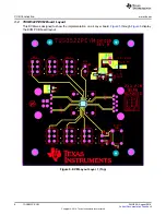
Page 8: ...ntation Feedback Copyright 2016 Texas Instruments Incorporated TUSB522P EVM 3 2 TUSB522P EVM Board Layout This EVM was designed to show the implementation on a 4 layer board Figure 5 through Figure 8 display the EVM PCB board layout Figure 5 EVM Layout Layer 1 Top ...

Page 9: ...www ti com PCB Construction 9 SLLU244 August 2016 Submit Documentation Feedback Copyright 2016 Texas Instruments Incorporated TUSB522P EVM Figure 6 EVM Layout Layer 2 GND ...

Page 10: ...PCB Construction www ti com 10 SLLU244 August 2016 Submit Documentation Feedback Copyright 2016 Texas Instruments Incorporated TUSB522P EVM Figure 7 EVM Layout Layer 3 VCC ...

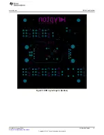
Page 11: ...www ti com PCB Construction 11 SLLU244 August 2016 Submit Documentation Feedback Copyright 2016 Texas Instruments Incorporated TUSB522P EVM Figure 8 EVM Layout Layer 4 Bottom ...

Page 12: ... C3 C4 C11 C12 0 1uF 2 2 C5 C6 10uF 3 4 C7 C8 C9 C10 1uF 4 2 C13 C14 0 01uF 5 1 C15 22uF 6 1 C16 22uF 7 1 D1 LED Green 0805 8 8 J1 J2 J3 J4 J5 J6 J7 J8 HDR3X2 1X 1 9 3 J9 J10 J11 HDR2X1 M 1 10 1 P1 USB3 0 Type B Receptacle 11 1 P2 USB3 Type A Receptacle 12 17 R1 R3 R4 R6 R7 R9 R10 R12 R13 R15 R16 R18 R19 R21 R22 R24 R25 1k 13 8 R2 R5 R8 R11 R14 R17 R20 R23 20k 14 1 R26 0 Ohm 15 1 R27 10k NO POP 16...

Page 13: ...ring the warranty period to the address designated by TI and that are determined by TI not to conform to such warranty If TI elects to repair or replace such EVM TI shall have a reasonable time to repair such EVM or provide replacements Repaired EVMs shall be warranted for the remainder of the original warranty period Replaced EVMs shall be warranted for a new full ninety 90 day warranty period 3 ...

Page 14: ... by Industry Canada to operate with the antenna types listed in the user guide with the maximum permissible gain and required antenna impedance for each antenna type indicated Antenna types not included in this list having a gain greater than the maximum gain indicated for that type are strictly prohibited for use with this device Concernant les EVMs avec antennes détachables Conformément à la rég...

Page 15: ... connecting any load to the EVM output If there is uncertainty as to the load specification please contact a TI field representative During normal operation even with the inputs and outputs kept within the specified allowable ranges some circuit components may have elevated case temperatures These components include but are not limited to linear regulators switching transistors pass transistors cu...

Page 16: ...F REMOVAL OR REINSTALLATION ANCILLARY COSTS TO THE PROCUREMENT OF SUBSTITUTE GOODS OR SERVICES RETESTING OUTSIDE COMPUTER TIME LABOR COSTS LOSS OF GOODWILL LOSS OF PROFITS LOSS OF SAVINGS LOSS OF USE LOSS OF DATA OR BUSINESS INTERRUPTION NO CLAIM SUIT OR ACTION SHALL BE BROUGHT AGAINST TI MORE THAN ONE YEAR AFTER THE RELATED CAUSE OF ACTION HAS OCCURRED 8 2 Specific Limitations IN NO EVENT SHALL T...

Page 17: ...esponsible for compliance with all legal regulatory and safety related requirements concerning its products and any use of TI components in its applications notwithstanding any applications related information or support that may be provided by TI Buyer represents and agrees that it has all the necessary expertise to create and implement safeguards which anticipate dangerous consequences of failur...

Page 18: ...Mouser Electronics Authorized Distributor Click to View Pricing Inventory Delivery Lifecycle Information Texas Instruments TUSB522PEVM ...

Reviews: