background image

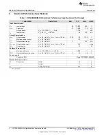
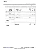
RADIO FREQUENCY REGULATORY COMPLIANCE INFORMATION FOR EVALUATION MODULES

Texas Instruments Incorporated (TI) evaluation boards, kits, and/or modules (EVMs) and/or accompanying hardware that is marketed, sold,
or loaned to users may or may not be subject to radio frequency regulations in specific countries.

General Statement for EVMs Not Including a Radio

For EVMs not including a radio and not subject to the U.S. Federal Communications Commission (FCC) or Industry Canada (IC)
regulations, TI intends EVMs to be used only for engineering development, demonstration, or evaluation purposes. EVMs are not finished
products typically fit for general consumer use. EVMs may nonetheless generate, use, or radiate radio frequency energy, but have not been
tested for compliance with the limits of computing devices pursuant to part 15 of FCC or the ICES-003 rules. Operation of such EVMs may
cause interference with radio communications, in which case the user at his own expense will be required to take whatever measures may
be required to correct this interference.

General Statement for EVMs including a radio

User Power/Frequency Use Obligations

: For EVMs including a radio, the radio included in such EVMs is intended for development and/or

professional use only in legally allocated frequency and power limits. Any use of radio frequencies and/or power availability in such EVMs
and their development application(s) must comply with local laws governing radio spectrum allocation and power limits for such EVMs. It is
the user’s sole responsibility to only operate this radio in legally acceptable frequency space and within legally mandated power limitations.
Any exceptions to this are strictly prohibited and unauthorized by TI unless user has obtained appropriate experimental and/or development
licenses from local regulatory authorities, which is the sole responsibility of the user, including its acceptable authorization.

U.S. Federal Communications Commission Compliance

For EVMs Annotated as FCC – FEDERAL COMMUNICATIONS COMMISSION Part 15 Compliant

Caution

This device complies with part 15 of the FCC Rules. Operation is subject to the following two conditions: (1) This device may not cause
harmful interference, and (2) this device must accept any interference received, including interference that may cause undesired operation.
Changes or modifications could void the user's authority to operate the equipment.

FCC Interference Statement for Class A EVM devices

This equipment has been tested and found to comply with the limits for a Class A digital device, pursuant to part 15 of the FCC Rules.
These limits are designed to provide reasonable protection against harmful interference when the equipment is operated in a commercial
environment. This equipment generates, uses, and can radiate radio frequency energy and, if not installed and used in accordance with the
instruction manual, may cause harmful interference to radio communications. Operation of this equipment in a residential area is likely to
cause harmful interference in which case the user will be required to correct the interference at its own expense.

FCC Interference Statement for Class B EVM devices

This equipment has been tested and found to comply with the limits for a Class B digital device, pursuant to part 15 of the FCC Rules.
These limits are designed to provide reasonable protection against harmful interference in a residential installation. This equipment
generates, uses and can radiate radio frequency energy and, if not installed and used in accordance with the instructions, may cause
harmful interference to radio communications. However, there is no guarantee that interference will not occur in a particular installation. If
this equipment does cause harmful interference to radio or television reception, which can be determined by turning the equipment off and
on, the user is encouraged to try to correct the interference by one or more of the following measures:

• Reorient or relocate the receiving antenna.

• Increase the separation between the equipment and receiver.

• Connect the equipment into an outlet on a circuit different from that to which the receiver is connected.

• Consult the dealer or an experienced radio/TV technician for help.

Industry Canada Compliance (English)

For EVMs Annotated as IC – INDUSTRY CANADA Compliant:

This Class A or B digital apparatus complies with Canadian ICES-003.

Changes or modifications not expressly approved by the party responsible for compliance could void the user’s authority to operate the
equipment.

Concerning EVMs Including Radio Transmitters

This device complies with Industry Canada licence-exempt RSS standard(s). Operation is subject to the following two conditions: (1) this
device may not cause interference, and (2) this device must accept any interference, including interference that may cause undesired
operation of the device.

Concerning EVMs Including Detachable Antennas

Under Industry Canada regulations, this radio transmitter may only operate using an antenna of a type and maximum (or lesser) gain
approved for the transmitter by Industry Canada. To reduce potential radio interference to other users, the antenna type and its gain should
be so chosen that the equivalent isotropically radiated power (e.i.r.p.) is not more than that necessary for successful communication.

This radio transmitter has been approved by Industry Canada to operate with the antenna types listed in the user guide with the maximum
permissible gain and required antenna impedance for each antenna type indicated. Antenna types not included in this list, having a gain
greater than the maximum gain indicated for that type, are strictly prohibited for use with this device.

Summary of Contents for UCC28880EVM-616

Page 1: ...Using the UCC28880EVM 616 User s Guide Literature Number SLUUB56A July 2014 Revised August 2014 ...

Page 2: ...igh side buck low power converters Additional features are low standby power and a minimum number of external components The PWM signal generation is based on a maximum constant ON time concept and each ON pulse is followed by a minimum OFF time to ensure the power MOSFET is not continuously driven in the ON state The PWM signal is AND gated with the signal from a current limiter The AND gated sig...

Page 3: ...Shutdown Controlled Start Up and Restart After Fault Protection CAUTION High voltage levels are present on the evaluation module whenever it is energized Proper precautions must be taken when working with the EVM The large bulk capacitors C1 and C2 must be completely discharged before the EVM can be handled Serious injury can occur if proper safety precautions are not followed 3 SLUUB56A July 2014...

Page 4: ...um output current VIN 85 V to 265 V 100 mA IOUT Output current range VIN 85 V to 265 V 0 100 mA VOUT_ripple Output voltage ripple VIN 85 V to 265 V IOUT 0 mA to 100 mA 200 mVpp POUT Output power VIN 85 V to 265 V 1 3 W Systems Characteristics h Maximum efficiency VIN 115 V 230 V IOUT 100 mA 80 82 TOP Operating temperature range VIN 85 V to 265 V IOUT 0 mA to 100 mA 0 25 40 C Environmental Conducte...

Page 5: ...o 265 V 100 mA Current IOUT Output Current Range VIN 85 V to 265 V 0 100 mA VOUT ripple Output Voltage Ripple VIN 85 V to 265 V IOUT 100 mA 150 mVpp POUT Output Power VIN 85 V to 265 V 0 43 W Systems Characteristics h Maximum Efficiency VIN 115 V 230 V IOUT 100 mA 62 61 TOP Operating VIN 85 V to 265 V IOUT 0 mA to 100 mA 0 25 40 C Temperature Range Environmental Conducted EMI Meets CISPR22B EN5502...

Page 6: ...VDC 100mA GND_IC 1 GND_IC 2 FB 3 VDD 4 HVIN 5 NC 6 DRAIN 8 U1 UCC28880D 1 2 P1 282841 2 JP1 FIT TP1 REMOVE Vo Pin2 to Pin1 5V 13V JP1 FIT REMOVE Vo Pin2 to Pin1 5V 13V 1mH L1 DANGER HIGH VOLTAGE Schematic www ti com 5 Schematic Figure 1 UCC28880EVM 616 Schematic 6 UCC28880EVM 616 High Side Buck Evaluation Module SLUUB56A July 2014 Revised August 2014 Submit Documentation Feedback Copyright 2014 Te...

Page 7: ...R DESCRIPTION NOTE JP1 Selecting feedback resistor values to select between 5 V and 13 V output Output is measured from pin 2 to pin 1 of P2 When the jumper is inserted the output is 5 V When left open the output is 13 V Table 4 UCC28880EVM 616 Test Points DESIGNATOR DESCRIPTION TP1 Buck switch node TP2 High voltage rectified DC TP3 GND TP4 GND TP5 VOUT Table 5 UCC28880EVM616 Board Connectors CONN...

Page 8: ...nt through the feedback and set to 100 µA on this board When the jumper JP1 is closed the resistor R4 is connected in parallel with resistor R3 and the output is set to 5 V To change either the output voltage or the feedback path current use the equations above There is a pre loaded resistor R5 which sets a pre load of 1 mA at the output when 13 V is selected With 5 V output the preload is 400 µA ...

Page 9: ...d to evaluate the UCC28880EVM 616 Start by applying a low DC voltage 15 V to 20 V into the AC input P1 When connected correctly the output voltage is regulated to 13 V positive with respect to GND Once correct output level is obtained increase the input voltage to the desired level Figure 2 UCC28880EVM 616 Test Setup 9 SLUUB56A July 2014 Revised August 2014 UCC28880EVM 616 High Side Buck Evaluatio...

Page 10: ...vely an electronic load may be used NOTE The output is not isolated from the AC and the electronic load must be capable of operating from a high voltage input Power Meter The power analyzer PM1 is capable of measuring low input current typically less than 100 µA and a long averaging mode if low power standby mode input power measurements are to be taken An example of such an analyzer is the Yokoga...

Page 11: ...2 82 9 12 61 40 632 79 8 12 6 51 794 80 9 12 59 59 922 80 6 12 58 70 1091 80 7 12 57 79 1221 81 3 12 56 89 1390 80 4 12 57 100 1554 80 9 Table 7 Efficiency and Regulation at 115 VAC for 13 V Output VO IO PIN EFFICIENCY 13 23 0 38 0 0 12 71 9 184 62 2 12 67 19 294 81 9 12 63 30 492 77 0 12 61 41 648 79 8 12 6 51 815 78 8 12 59 61 986 77 9 12 58 69 1116 77 8 12 57 80 1284 78 3 12 57 91 1448 79 0 12 ...

Page 12: ...9 405 63 4 4 34 70 481 63 2 4 33 81 555 63 2 4 32 89 613 62 7 4 31 100 689 62 6 Table 9 Efficiency and Regulation at 230 VAC for 5 V Output VO IO PIN EFFICIENCY 6 26 0 24 0 0 4 51 10 81 55 7 4 44 19 140 60 3 4 4 29 214 59 6 4 38 39 275 62 1 4 37 49 344 62 2 4 36 60 418 62 6 4 35 70 492 61 9 4 34 78 549 61 7 4 34 89 625 61 8 4 33 100 703 61 6 Figure 6 Efficiency for 5 V output Figure 5 Regulation f...

Page 13: ... 3 Switching Waveforms Figure 9 VD4 at 115 VAC In 4 27 VOUT 75 Ω Figure 10 VD4 at 115 VAC In 4 27 VOUT 75 Ω Figure 11 VD4 at 230 VAC In 4 27 VOUT 75 Ω Figure 12 VD4 at 230 VAC In 4 27 VOUT 75 Ω 13 SLUUB56A July 2014 Revised August 2014 UCC28880EVM 616 High Side Buck Evaluation Module Submit Documentation Feedback Copyright 2014 Texas Instruments Incorporated ...

Page 14: ...mA Figure 14 VD4 at 115 VAC In 12 55 VOUT 100 mA Figure 15 VD4 at 230 VAC In 12 55 VOUT 100 mA Figure 16 VD4 at 230 VAC In 12 60 VOUT 100 mA 14 UCC28880EVM 616 High Side Buck Evaluation Module SLUUB56A July 2014 Revised August 2014 Submit Documentation Feedback Copyright 2014 Texas Instruments Incorporated ...

Page 15: ...how the design of the UCC2880EVM 616 printed circuit board Figure 17 UCC28880EVM 616 Assembly top view Figure 18 UCC28880EVM 616 Layout top layer 15 SLUUB56A July 2014 Revised August 2014 UCC28880EVM 616 High Side Buck Evaluation Module Submit Documentation Feedback Copyright 2014 Texas Instruments Incorporated ...

Page 16: ... 08 mm TH TE Connectivity 282841 2 1 R1 Resistor 8 2 Ω 5 3 W fusible TH Bourns PWR4522AS8R20JA 1 R2 Resistor 10 0 kΩ 1 0 125 W 0805 Panasonic ERJ 6ENF1002V 1 R3 Resistor 121 kΩ 1 0 125 W 0805 Panasonic ERJ 6ENF1213V 1 R4 Resistor 57 6 kΩ 1 0 125 W 0805 Panasonic ERJ 6ENF5762V 1 R5 Resistor 12 1 kΩ 1 0 125 W 0805 Panasonic ERJ 6ENF1212V 1 SH JP1 Shunt 100 millimeter flash gold black Sullins Connect...

Page 17: ...ndling and use of EVMs and if applicable compliance in all respects with such laws and regulations 10 User has sole responsibility to ensure the safety of any activities to be conducted by it and its employees affiliates contractors or designees with respect to handling and using EVMs Further user is responsible to ensure that any interfaces electronic and or mechanical between EVMs and any human ...

Page 18: ...This equipment generates uses and can radiate radio frequency energy and if not installed and used in accordance with the instruction manual may cause harmful interference to radio communications Operation of this equipment in a residential area is likely to cause harmful interference in which case the user will be required to correct the interference at its own expense FCC Interference Statement ...

Page 19: ...érieur au gain maximal indiqué sont strictement interdits pour l exploitation de l émetteur Mailing Address Texas Instruments Post Office Box 655303 Dallas Texas 75265 Copyright 2014 Texas Instruments Incorporated spacer Important Notice for Users of EVMs Considered Radio Frequency Products in Japan EVMs entering Japan are NOT certified by TI as conforming to Technical Regulations of Radio Law of ...

Page 20: ...esponsible for compliance with all legal regulatory and safety related requirements concerning its products and any use of TI components in its applications notwithstanding any applications related information or support that may be provided by TI Buyer represents and agrees that it has all the necessary expertise to create and implement safeguards which anticipate dangerous consequences of failur...

Page 21: ...Mouser Electronics Authorized Distributor Click to View Pricing Inventory Delivery Lifecycle Information Texas Instruments UCC28880EVM 616 ...

Reviews: