background image

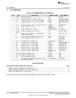
Canada Industry Canada Compliance (French)

Cet appareil numérique de la classe A ou B est conforme à la norme NMB-003 du Canada

Les changements ou les modifications pas expressément approuvés par la partie responsable de la conformité ont pu vider l’autorité de
l'utilisateur pour actionner l'équipement.

Concernant les EVMs avec appareils radio

Le présent appareil est conforme aux CNR d'Industrie Canada applicables aux appareils radio exempts de licence. L'exploitation est
autorisée aux deux conditions suivantes : (1) l'appareil ne doit pas produire de brouillage, et (2) l'utilisateur de l'appareil doit accepter tout
brouillage radioélectrique subi, même si le brouillage est susceptible d'en compromettre le fonctionnement.

Concernant les EVMs avec antennes détachables

Conformément à la réglementation d'Industrie Canada, le présent émetteur radio peut fonctionner avec une antenne d'un type et d'un gain
maximal (ou inférieur) approuvé pour l'émetteur par Industrie Canada. Dans le but de réduire les risques de brouillage radioélectrique à
l'intention des autres utilisateurs, il faut choisir le type d'antenne et son gain de sorte que la puissance isotrope rayonnée équivalente
(p.i.r.e.) ne dépasse pas l'intensité nécessaire à l'établissement d'une communication satisfaisante.

Le présent émetteur radio a été approuvé par Industrie Canada pour fonctionner avec les types d'antenne énumérés dans le manuel
d’usage et ayant un gain admissible maximal et l'impédance requise pour chaque type d'antenne. Les types d'antenne non inclus dans
cette liste, ou dont le gain est supérieur au gain maximal indiqué, sont strictement interdits pour l'exploitation de l'émetteur.

Mailing Address: Texas Instruments, Post Office Box 655303, Dallas, Texas 75265

Copyright © 2014, Texas Instruments Incorporated

spacer

Important Notice for Users of EVMs Considered “Radio Frequency Products” in Japan

EVMs entering Japan are NOT certified by TI as conforming to Technical Regulations of Radio Law of Japan.

If user uses EVMs in Japan, user is required by Radio Law of Japan to follow the instructions below with respect to EVMs:

1.

Use EVMs in a shielded room or any other test facility as defined in the notification #173 issued by Ministry of Internal Affairs and
Communications on March 28, 2006, based on Sub-section 1.1 of Article 6 of the Ministry’s Rule for Enforcement of Radio Law of
Japan,

2.

Use EVMs only after user obtains the license of Test Radio Station as provided in Radio Law of Japan with respect to EVMs, or

3.

Use of EVMs only after user obtains the Technical Regulations Conformity Certification as provided in Radio Law of Japan with respect
to EVMs. Also, do not transfer EVMs, unless user gives the same notice above to the transferee. Please note that if user does not
follow the instructions above, user will be subject to penalties of Radio Law of Japan.

http://www.tij.co.jp

【無線電波を送信する製品の開発キットをお使いになる際の注意事項】 本開発キットは技術基準適合証明を受けておりません。 本製品の
ご使用に際しては、電波法遵守のため、以下のいずれかの措置を取っていただく必要がありますのでご注意ください。

1.

電波法施行規則第

6

条第

1

項第

1

号に基づく平成

18

3

28

日総務省告示第

173

号で定められた電波暗室等の試験設備でご使用いただく。

2.

実験局の免許を取得後ご使用いただく。

3.

技術基準適合証明を取得後ご使用いただく。。

なお、本製品は、上記の「ご使用にあたっての注意」を譲渡先、移転先に通知しない限り、譲渡、移転できないものとします

上記を遵守頂けない場合は、電波法の罰則が適用される可能性があることをご留意ください。

日本テキサス・インスツルメンツ株式会社

東京都新宿区西新宿6丁目24番1号

西新宿三井ビル

http://www.tij.co.jp

Texas Instruments Japan Limited

(address) 24-1, Nishi-Shinjuku 6 chome, Shinjuku-ku, Tokyo, Japan

Summary of Contents for UCC28880EVM-616

Page 1: ...Using the UCC28880EVM 616 User s Guide Literature Number SLUUB56A July 2014 Revised August 2014 ...

Page 2: ...igh side buck low power converters Additional features are low standby power and a minimum number of external components The PWM signal generation is based on a maximum constant ON time concept and each ON pulse is followed by a minimum OFF time to ensure the power MOSFET is not continuously driven in the ON state The PWM signal is AND gated with the signal from a current limiter The AND gated sig...

Page 3: ...Shutdown Controlled Start Up and Restart After Fault Protection CAUTION High voltage levels are present on the evaluation module whenever it is energized Proper precautions must be taken when working with the EVM The large bulk capacitors C1 and C2 must be completely discharged before the EVM can be handled Serious injury can occur if proper safety precautions are not followed 3 SLUUB56A July 2014...

Page 4: ...um output current VIN 85 V to 265 V 100 mA IOUT Output current range VIN 85 V to 265 V 0 100 mA VOUT_ripple Output voltage ripple VIN 85 V to 265 V IOUT 0 mA to 100 mA 200 mVpp POUT Output power VIN 85 V to 265 V 1 3 W Systems Characteristics h Maximum efficiency VIN 115 V 230 V IOUT 100 mA 80 82 TOP Operating temperature range VIN 85 V to 265 V IOUT 0 mA to 100 mA 0 25 40 C Environmental Conducte...

Page 5: ...o 265 V 100 mA Current IOUT Output Current Range VIN 85 V to 265 V 0 100 mA VOUT ripple Output Voltage Ripple VIN 85 V to 265 V IOUT 100 mA 150 mVpp POUT Output Power VIN 85 V to 265 V 0 43 W Systems Characteristics h Maximum Efficiency VIN 115 V 230 V IOUT 100 mA 62 61 TOP Operating VIN 85 V to 265 V IOUT 0 mA to 100 mA 0 25 40 C Temperature Range Environmental Conducted EMI Meets CISPR22B EN5502...

Page 6: ...VDC 100mA GND_IC 1 GND_IC 2 FB 3 VDD 4 HVIN 5 NC 6 DRAIN 8 U1 UCC28880D 1 2 P1 282841 2 JP1 FIT TP1 REMOVE Vo Pin2 to Pin1 5V 13V JP1 FIT REMOVE Vo Pin2 to Pin1 5V 13V 1mH L1 DANGER HIGH VOLTAGE Schematic www ti com 5 Schematic Figure 1 UCC28880EVM 616 Schematic 6 UCC28880EVM 616 High Side Buck Evaluation Module SLUUB56A July 2014 Revised August 2014 Submit Documentation Feedback Copyright 2014 Te...

Page 7: ...R DESCRIPTION NOTE JP1 Selecting feedback resistor values to select between 5 V and 13 V output Output is measured from pin 2 to pin 1 of P2 When the jumper is inserted the output is 5 V When left open the output is 13 V Table 4 UCC28880EVM 616 Test Points DESIGNATOR DESCRIPTION TP1 Buck switch node TP2 High voltage rectified DC TP3 GND TP4 GND TP5 VOUT Table 5 UCC28880EVM616 Board Connectors CONN...

Page 8: ...nt through the feedback and set to 100 µA on this board When the jumper JP1 is closed the resistor R4 is connected in parallel with resistor R3 and the output is set to 5 V To change either the output voltage or the feedback path current use the equations above There is a pre loaded resistor R5 which sets a pre load of 1 mA at the output when 13 V is selected With 5 V output the preload is 400 µA ...

Page 9: ...d to evaluate the UCC28880EVM 616 Start by applying a low DC voltage 15 V to 20 V into the AC input P1 When connected correctly the output voltage is regulated to 13 V positive with respect to GND Once correct output level is obtained increase the input voltage to the desired level Figure 2 UCC28880EVM 616 Test Setup 9 SLUUB56A July 2014 Revised August 2014 UCC28880EVM 616 High Side Buck Evaluatio...

Page 10: ...vely an electronic load may be used NOTE The output is not isolated from the AC and the electronic load must be capable of operating from a high voltage input Power Meter The power analyzer PM1 is capable of measuring low input current typically less than 100 µA and a long averaging mode if low power standby mode input power measurements are to be taken An example of such an analyzer is the Yokoga...

Page 11: ...2 82 9 12 61 40 632 79 8 12 6 51 794 80 9 12 59 59 922 80 6 12 58 70 1091 80 7 12 57 79 1221 81 3 12 56 89 1390 80 4 12 57 100 1554 80 9 Table 7 Efficiency and Regulation at 115 VAC for 13 V Output VO IO PIN EFFICIENCY 13 23 0 38 0 0 12 71 9 184 62 2 12 67 19 294 81 9 12 63 30 492 77 0 12 61 41 648 79 8 12 6 51 815 78 8 12 59 61 986 77 9 12 58 69 1116 77 8 12 57 80 1284 78 3 12 57 91 1448 79 0 12 ...

Page 12: ...9 405 63 4 4 34 70 481 63 2 4 33 81 555 63 2 4 32 89 613 62 7 4 31 100 689 62 6 Table 9 Efficiency and Regulation at 230 VAC for 5 V Output VO IO PIN EFFICIENCY 6 26 0 24 0 0 4 51 10 81 55 7 4 44 19 140 60 3 4 4 29 214 59 6 4 38 39 275 62 1 4 37 49 344 62 2 4 36 60 418 62 6 4 35 70 492 61 9 4 34 78 549 61 7 4 34 89 625 61 8 4 33 100 703 61 6 Figure 6 Efficiency for 5 V output Figure 5 Regulation f...

Page 13: ... 3 Switching Waveforms Figure 9 VD4 at 115 VAC In 4 27 VOUT 75 Ω Figure 10 VD4 at 115 VAC In 4 27 VOUT 75 Ω Figure 11 VD4 at 230 VAC In 4 27 VOUT 75 Ω Figure 12 VD4 at 230 VAC In 4 27 VOUT 75 Ω 13 SLUUB56A July 2014 Revised August 2014 UCC28880EVM 616 High Side Buck Evaluation Module Submit Documentation Feedback Copyright 2014 Texas Instruments Incorporated ...

Page 14: ...mA Figure 14 VD4 at 115 VAC In 12 55 VOUT 100 mA Figure 15 VD4 at 230 VAC In 12 55 VOUT 100 mA Figure 16 VD4 at 230 VAC In 12 60 VOUT 100 mA 14 UCC28880EVM 616 High Side Buck Evaluation Module SLUUB56A July 2014 Revised August 2014 Submit Documentation Feedback Copyright 2014 Texas Instruments Incorporated ...

Page 15: ...how the design of the UCC2880EVM 616 printed circuit board Figure 17 UCC28880EVM 616 Assembly top view Figure 18 UCC28880EVM 616 Layout top layer 15 SLUUB56A July 2014 Revised August 2014 UCC28880EVM 616 High Side Buck Evaluation Module Submit Documentation Feedback Copyright 2014 Texas Instruments Incorporated ...

Page 16: ... 08 mm TH TE Connectivity 282841 2 1 R1 Resistor 8 2 Ω 5 3 W fusible TH Bourns PWR4522AS8R20JA 1 R2 Resistor 10 0 kΩ 1 0 125 W 0805 Panasonic ERJ 6ENF1002V 1 R3 Resistor 121 kΩ 1 0 125 W 0805 Panasonic ERJ 6ENF1213V 1 R4 Resistor 57 6 kΩ 1 0 125 W 0805 Panasonic ERJ 6ENF5762V 1 R5 Resistor 12 1 kΩ 1 0 125 W 0805 Panasonic ERJ 6ENF1212V 1 SH JP1 Shunt 100 millimeter flash gold black Sullins Connect...

Page 17: ...ndling and use of EVMs and if applicable compliance in all respects with such laws and regulations 10 User has sole responsibility to ensure the safety of any activities to be conducted by it and its employees affiliates contractors or designees with respect to handling and using EVMs Further user is responsible to ensure that any interfaces electronic and or mechanical between EVMs and any human ...

Page 18: ...This equipment generates uses and can radiate radio frequency energy and if not installed and used in accordance with the instruction manual may cause harmful interference to radio communications Operation of this equipment in a residential area is likely to cause harmful interference in which case the user will be required to correct the interference at its own expense FCC Interference Statement ...

Page 19: ...érieur au gain maximal indiqué sont strictement interdits pour l exploitation de l émetteur Mailing Address Texas Instruments Post Office Box 655303 Dallas Texas 75265 Copyright 2014 Texas Instruments Incorporated spacer Important Notice for Users of EVMs Considered Radio Frequency Products in Japan EVMs entering Japan are NOT certified by TI as conforming to Technical Regulations of Radio Law of ...

Page 20: ...esponsible for compliance with all legal regulatory and safety related requirements concerning its products and any use of TI components in its applications notwithstanding any applications related information or support that may be provided by TI Buyer represents and agrees that it has all the necessary expertise to create and implement safeguards which anticipate dangerous consequences of failur...

Page 21: ...Mouser Electronics Authorized Distributor Click to View Pricing Inventory Delivery Lifecycle Information Texas Instruments UCC28880EVM 616 ...

Reviews: