


+
($
=
8
176
4
2 +
4
3
8
176
=
4
2 +
4
3
4
2
×
8
($
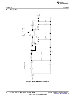
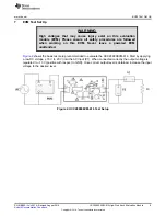
Circuit Description
The UCC28880EVM-616 is configured as a non-isolated AC-to-DC high-side buck converter with direct
feedback. The output voltage OUT is referenced to the GND node, which is referenced to the negative
high voltage node N. The potential difference between these nodes is equivalent to the voltage drop in
diode D2. The output voltage is positive with respect to the GND node. The output voltage at OUT can be
selected to be either ~5 V (typical) or ~13 V (typical) with the jumper JP1. See
for jumper settings
to select between the two output voltage levels.
AC input voltage can be fed to the AC input nodes L and N in connector P1. When connecting AC input to
P1 it does not matter which way line and neutral are connected to the P1 nodes. When connecting DC
input to P1, please verify that polarity is correct, L is the positive node and N the negative node.
The feedback path, consisting of resistors R2 and R3, diode D5 and capacitor C4, sets the output voltage
to ~13 V by default when the jumper JP1 is open. The diode D5 is identical to D4, and their voltage drops
compensate each other. The feedback is sampling the output voltage level to capacitor C4 during the off
state of the integrated HV FET of the UCC28880 and the output voltage is set by the resistors R2 and R3
following the equation:
(1)
where V
OUT
is the output voltage and V
FB
= 1.0 V is the voltage level at the feedback pin. The current
through the external feedback path is set by the total resistance between OUT and GND nodes (resistors
R2 through R3):
(2)
where I
FB
is the current through the feedback and set to ~100 µA on this board.
When the jumper JP1 is closed, the resistor R4 is connected in parallel with resistor R3, and the output is
set to ~5 V. To change either the output voltage or the feedback path current, use the equations above.
There is a pre-loaded resistor (R5), which sets a pre-load of ~1 mA at the output when 13 V is selected.
With 5 V output, the preload is ~400 µA. A load of up to 100 mA can be applied to the output.
The design of UCC28880EVM-616 is optimized for 13-V output setting. For 5-V setting, there is additional
room for optimization when factors such as audible noise, output voltage ripple, stand-by power etc are
considered. The value of the bootstrap capacitor (C4), the impedance of the feedback divider network (R4,
R3, R2), and output capacitor (C5) are especially critical. The RC time constant of the bootstrap capacitor
and feedback resistor divider network influences voltage on the FB pin, which in turn, influences the burst
pattern of switching pulses in the device. By adjusting these components the frequency of the burst
pattern can be manipulated higher or lower. This is an effective way to address audible noise emanating
from the magnetics and capacitors in the system. A higher RC time constant reduces the frequency of
occurrence of burst pulses, which increases the output voltage ripple unless the value of output capacitor
is also increased alongside. A lower-time constant increases the frequency of the burst pattern, but a
smaller resistor divider impedance increases the stand-by power consumption. These trade-offs have to
be considered when designing the power supply.
8
UCC28880EVM-616 High-Side Buck Evaluation Module
SLUUB56A – July 2014 – Revised August 2014
Copyright © 2014, Texas Instruments Incorporated


