background image

SLUU085 – November 2001

12

UCC3580EVM

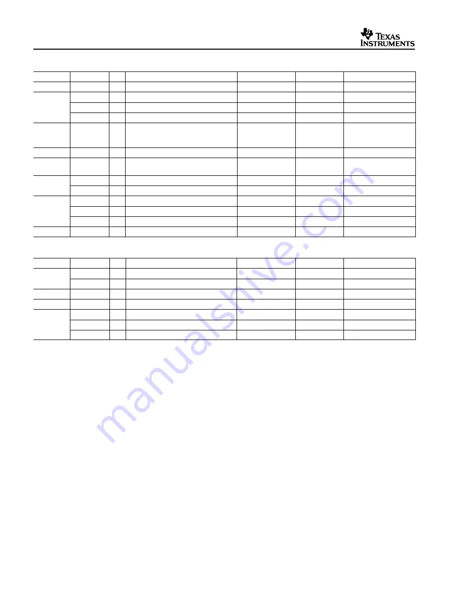
Table 3. Conversion From Active Clamp to Hard-Switched Configuration: Remove List

Ref Des

Qty

Description

MFG

Size

Part Number

Capacitor

C6, C11

2

Ceramic, 0.1 

µ

F, 50 V

Panasonic

5 mm

ECU–S1H104KBB

D5, D10

2

Switching, 75 mA, 75 V

DO–35

1N4148

Diode

D7, D11

2

Schottky, 1 A, 40 V

DO–41

1N5819

Diode

D16

1

Ultra Fast, 4 A, 400 V

DO–201AD

MUR460

Heatsink

HS2

1

For QA, 13 C/W. Remove as an as-
sembly with QA and all of the mounting
hardware attached to HS2.

Thermalloy

24.38 mm

6021PB

Choke

L3

1

E25/10/6–3F3 core, 10-pins, 16 

µ

H

Century Magnetics

5.1X15.6 mm

CMI–2408

MOSFET

QA

1

400 V, 0.55 

, 10 A (removed with

HS2)

IR

TO–220AB

IRF740

Transistor

Q2

1

NPN, 40 V, 200 mA

TO–226AA

2N3904

Transistor

Q4

1

PNP, 40 V, 200 mA

TO–226AA

2N3906

R5

1

30 

, 1/4 w, 5%

10.16 mm

Resistor

R15

1

1/4 W, 4.7 k

, 5%

10.16 mm

Resistor

R23

1

1/4 W, 10 k

, 5%

10.16 mm

Gate

T1

1

xfmr, 8-pins

Coiltronics

2.5X8 mm

CTX08–14086–X1

Table 4. Conversion From Active Clamp to Hard-Switched Configuration: Add List

Ref Des

Qty

Description

MFG

Size

Part Number

Capacitor

C20

1

Ceramic disk, 390 pF, 1 kV

Panasonic

5 mm

ECK–D3A391KBN

Capacitor

C30

1

Polyester, 0.01 

µ

F, 100 V

Panasonic

5 mm

ECQ–E1103KF

Diode

D8, D12

2

Ultra fast, 1 A, 600 V

DO–41

MUR160

Jumper

L3

1

Pin 1 to pin 4, 20AWG, insulated

14 mm

R9

1

5 W, wire, vertical, 1 k

, 5%

Ohmite

5 mm

TWM–5J1K0

Resistor

R25

1

5 W, wire, vertical, 6.8 k

, 5%

Ohmite

5 mm

TWM–5J6K8

Resistor

R31

1

5 W, wire, vertical, 4.7 

, 5%

Ohmite

5 mm

TWM–5J4R7

Summary of Contents for UCC3580EVM

Page 1: ...User Guide 1 UCC3580EVM Flyback Converters Active Clamp vs Hard Switched Evaluation Board and List of Materials User s Guide ...

Page 2: ...e handling or use of the goods Please be aware that the products received may not be regulatory compliant or agency certified FCC UL CE etc Due to the open construction of the product it is the user s responsibility to take any and all appropriate precautions with regard to electrostatic discharge EXCEPT TO THE EXTENT OF THE INDEMNITY SET FORTH ABOVE NEITHER PARTY SHALL BE LIABLE TO THE OTHER FOR ...

Page 3: ...put If there is uncertainty as to the load specification please contact a TI field representative During normal operation some circuit components may have case temperatures greater than 60 C The EVM is designed to operate properly with certain components above 125 C as long as the input and output ranges are maintained These components include but are not limited to linear regulators switching tra...

Page 4: ...ion 11 6 Traces and Silkscreen 13 6 1 Traces 13 6 2 Silkscreen 14 7 Reference 14 Figures 1 Recommended Test Setup for the UCC3580 Flyback Evaluation Board 7 2 Flyback Converter Populated for Active Clamp Operation 8 3 Flyback Converter Populated for Hard Switched Operation 11 4 UCC3580EVM Layout Top Traces 13 5 UCC3580EVM Layout Bottom Traces 13 6 UCC3580EVM Silk Screen only top layer has a silk s...

Page 5: ...down and soft restart D Low supply current 160 µA startup 2 5 mA operation 3 Description 3 1 Operating Guidelines WARNING DANGER HIGH VOLTAGE This evaluation board is intended for professional use only It has exposed high voltages Do not operate this board without proper isolation and high voltage high current safety practices Refer to the recommended test setup as shown in Figure 1 and the test p...

Page 6: ... hard switched configuration and it is thus over sized for active clamp operation The thermal resistance of HS1 is 6 5 C W which is required for hard switched operation In contrast heat sink HS1 only needs a thermal resistance of 10 C W for active clamp operation which was verified in the laboratory Thus transistor QM operates more efficiently and it requires a smaller heat sink in the active clam...

Page 7: ...ints Test Point Signal Name Voltage Range GND REF Measurement TP1 GND2 SEC Secondary ground TP2 12 V 12 V SEC 12 V observe relative to TP1 TP3 TP4 TP5 12 V 0 1 VAC SEC Injection and observation points for control loop Refer to 1 TP6 TP7 TP8 12 V 50 V 50 V SEC Differentially observe V D17 between TP6 and TP8 Differentially observe snubber power between TP6 and TP7 TP9 PRI GND PRI Primary ground for...

Page 8: ...6 SOURCE TP18 DRAIN C25 0 068µF 400V TP17 BULK 24 TURNS 158µH TP20 BULK C7 1000µF TP19 TPI GND R1 68k 1W D2 1N5406 D1 1N5406 D4 1N5406 D3 1N5406 C2 4700pF 250V C1 4700pF 250V J1 1 CHASSIS 1 4 5 8 C4 0 1µF 250V C5 0 1µF 250V L1 18µH R2 470k C3 0 1µF 250V F1 3A J1 3 LINE J1 2 NEUTRAL 13 14 3 TURNS 2 C34 180µF C33 180µF C32 180µF C31 180µF R31 NOT USED HS3 D17 MBRF2545CT C30 NOT USED TP8 ANODE TP6 CA...

Page 9: ... pF 250 Vac Panasonic 10 mm ECK DNA102MB C28 1 Ceramic 4 7 nF 50 V Panasonic 2 5 mm ECU S1H472KBA C29 1 Ceramic 470 pF 50 V Panasonic 7 5 mm ECU S1H471JCA C31 C34 4 Os Con 180 µF 20 V Sanyo 5 mm 20SP180M D1 D4 4 General Purpose 3 A 600 V DO 201AD 1N5406 D5 D10 D13 3 Switching 75 mA 75 V DO 35 1N4148 Diode D6 D7 D9 D11 4 Schottky 1 A 40 V DO 41 1N5819 Diode D14 1 Zener 15 V 1 W DO 41 1N4744A D15 1 ...

Page 10: ... 1 10 16 mm R10 1 1 4 W 20 0 kΩ 1 10 16 mm R11 1 1 4 W 511 kΩ 1 10 16 mm R12 R23 2 1 4 W 10 kΩ 5 10 16 mm R13 1 1 4 W 1 62 kΩ 1 10 16 mm Resistor R14 1 1 4 W 33 2 kΩ 1 10 16 mm Resistor R15 1 1 4 W 4 7 kΩ 5 10 16 mm R16 1 1 4 W 3 32 kΩ 1 10 16 mm R17 1 1 4 W 130 kΩ 1 10 16 mm R18 1 1 4 W 4 7 kΩ 5 10 16 mm R19 1 1 4 W 15 Ω 5 10 16 mm R21 1 1 4 W 1 kΩ 1 10 16 mm R22 R32 2 1 4 W 20 Ω 5 10 16 mm R24 1...

Page 11: ...RAIN C25 0 068µF 400V TP17 BULK 24 TURNS 158µH TP20 BULK C7 1000µF TP19 TPI GND R1 68k 1W D2 1N5406 D1 1N5406 D4 1N5406 D3 1N5406 C2 4700pF 250V C1 4700pF 250V J1 1 CHASSIS C4 0 1µF 250V C5 0 1µF 250V L1 18µH R2 470k C3 0 1µF 250V F1 3A J1 3 LINE J1 2 NEUTRAL 13 14 3 TURNS 2 C34 180µF C33 180µF C32 180µF C31 180µF R31 4 7 3W HS3 D17 MBRF2545CT C30 10nF 100V TP8 ANODE TP6 CATHODE TP7 SNUB TP12 12V ...

Page 12: ...d with HS2 IR TO 220AB IRF740 Transistor Q2 1 NPN 40 V 200 mA TO 226AA 2N3904 Transistor Q4 1 PNP 40 V 200 mA TO 226AA 2N3906 R5 1 30 Ω 1 4 w 5 10 16 mm Resistor R15 1 1 4 W 4 7 kΩ 5 10 16 mm Resistor R23 1 1 4 W 10 kΩ 5 10 16 mm Gate T1 1 xfmr 8 pins Coiltronics 2 5X8 mm CTX08 14086 X1 Table 4 Conversion From Active Clamp to Hard Switched Configuration Add List Ref Des Qty Description MFG Size Pa...

Page 13: ...November 2001 13 UCC3580EVM 6 Traces and silkscreen Figures 4 5 and 6 show the traces and silkscreen for the UCC3580EVM 6 1 Traces Figure 4 UCC3580EVM Layout Top Traces Figure 5 UCC3580EVM Layout Bottom Traces ...

Page 14: ...UCC3580EVM Silk Screen only top layer has a silk screen 7 Reference 1 R B Ridley Switching power supply design information design tips frequency response analyzers and educational material for power supplies See web site located at http www ridleyengineering com ...

Page 15: ...nt that any license either express or implied is granted under any TI patent right copyright mask work right or other TI intellectual property right relating to any combination machine or process in which TI products or services are used Information published by TI regarding third party products or services does not constitute a license from TI to use such products or services or a warranty or end...

Reviews: