L M K 0 4 9 0 6 E V A L U A T I O N B O A R D O P E R A T I N G I N S T R U C T I O N S
SNAU126
24
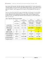
Case 4 shows 0-Delay mode with CLKout divider not equal to the PLL2_P value; however the
CLKout frequency will be less than the current phase detector frequency. This requires PLL2_R
to be increased from a value of 1 to 2 to reduce the PLL2 phase detector frequency from 122.88
MHz to 61.44 MHz. Now the adjusted VCO frequency can be programmed to allow PLL2 to
lock.
In any case where the actual VCO frequency and the display VCO frequency are not equal the
user is required to manually update the PLL2_N_CAL register with the PLL2_N value to be
used as if the device were operating in the non-0-Delay mode. Once this update has been
performed, Ctrl-L will reload the part and cause the VCO calibration to occur with the proper
PLL2_N_CAL value.
Table 7 - Single PLL 0-Delay Operation Examples
Case 1:
Default Mode
No 0-Delay
Case 2:
Default 0-Delay
Mode
(CLKout4 =
1474.56 MHz)
Case 3:
Default 0-Delay
Mode (Updated
CLKout4 =
245.76 MHz)
Case 4:
Default 0-Delay
Mode (Updated
CLKout4 =
61.44 MHz)
Actual PLL2
VCO Frequency
2949.12 MHz
2949.12 MHz
2949.12 MHz
2949.12 MHz
Reported PLL2
VCO Frequency
2949.12 MHz
2949.12 MHz
491.52 MHz
122.88 MHz
PLL2_R
1
1
1
2
PLL2_N
12
12
2
1
PLL2_N_CAL
12
12
12
24
PLL2_P (Pre-N)
2
2
2
2
PLL2 VCO Divider
Bypassed
Bypassed
Bypassed
Bypassed
CLKout8 Divide
12
2
12
48
Actual CLKout8
Output Frequency
245.76
1474.56 MHz
245.76 MHz
61.44 MHz
Reported CLKout8
Output Frequency
245.76
1474.56 MHz
40.96 MHz
2.56 MHz


