
THCV235_THCV236_Rev.3.40_E
Copyright
©
2016 THine Electronics, Inc.
THine Electronics, Inc.
1/68
Security E
THCV235 and THCV236
SerDes transmitter and receiver with bi-directional transceiver
General Description
The THCV235 and THCV236 are designed to
support video data transmission between the host and
display.
One high-speed lane can carry up to 32bit data and
3bits of synchronizing signals at a pixel clock
frequency from 6MHz to 160MHz by converting
RGB444 to YCbCr422.
The chipset, which has one high-speed data lane,
can transmit video data up to 1080p/60Hz.
The maximum serial data rate is 4.00Gbps/lane.
Features
Color depth selectable:24/32bit
RGB
YCbCr422 color space conversion
function
Wide frequency range
AC coupling for high-speed lanes
CDR requires no external frequency reference
Wide range supply voltage from 1.7V to 3.6V
Additional spread spectrum on data stream
2-wire serial interface bridge function(400kbps)
Remote side GPIO control and monitoring
Low speed data bridge function
QFN64(9mm x 9mm) with exposed pad ground
V-by-One
®
HS standard version1.4 compliant
EU RoHS compliant
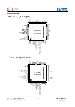
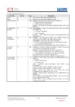
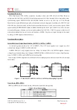
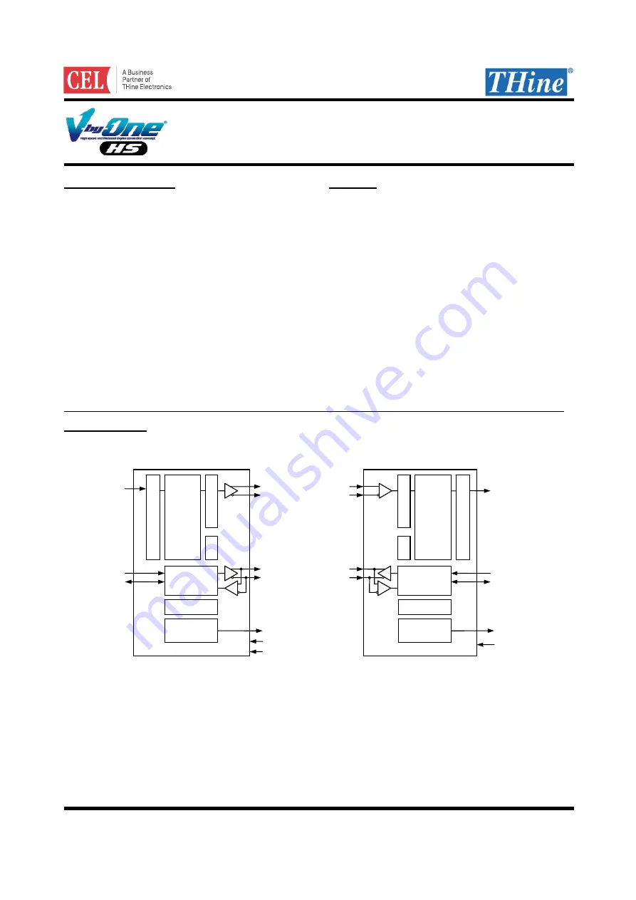
Block Diagram
THCV236
CDR
Controls
Formatte
r
YCbCr to
RGB
D31-D0
HSYNC
VSYNC
DE
CLKOUT
Settings
2-wire I/F
SDA/SCL
RXP
RXN
Deser
ializer
RCMP
RCMN
LV
CMOS o
utput
THCV235
LV
CMOS input
PLL
Controls
Formatte
r
RGB to
YCbC
r
D31-D0
HSYNC
VSYNC
DE
CLKIN
Settings
2-wire I/F
SDA/SCL
TXP
TXN
Ser
ializer
OSC
TCMP
TCMN
LDO
OSC
LDO
CAPOUT
CAPINA
CAPINP
CAPOUT
CAPINA


