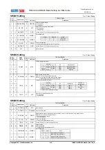
DRVSEL
1
H
9
RX DRVSEL
SW201 Setting
SW
Pin#
*
Def.
NodeName
THC63LVD824
IC
Pin#
PinName
* Def. : Default Setting
Description
Output Driverbility Select.
H : High power,
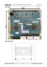
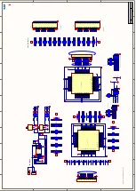
THEVA12LVDR820 Mode Setting & LVDS-Cable
THine Electronics, Inc.
2011/04/14
L
3
L
RX TESTO
Ground Pins for TTL outputs and digital circuitry.
Pixel Data Mode.
4
L
RX MODE1
5
L
RX R/F
8
DRVSEL
2
H
1
H
9
RX DRVSEL
H : High power,
L : Low power.
Mode
6
MODE1
7
Output Clock Triggering Edge Select.
H : Rising edge,
L : Falling edge.
R/F
MODE1
Dual Link
MODE0
Single Link
L
L
GND
MODE0
H
5
RX MODE0
Non Connected.
-
SW202 Setting
RX /PD
SW
7
L
RX TEST1
H
8
6
H
*
Node
Ground Pins for TTL outputs and digital circuitry.
H : Normal operation,
L : Power down (all outputs are pulled to ground)
* Def. : Default Setting
IC
THC63LVD823B
4
3
/PDWN
GND
N/C
-
1
2
3
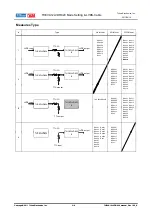
SW
Pin#
H
Def.
L
Node
Name
VIMM
Mapping Mode
1
MAP
14
IC
Pin#
Description
Mapping MODE2
H(open)
L
LVDS mapping table select.
3
H(open)
L
DDR function is active when
RS
SW-Pin#
L
H(open) H(open)
H(open)
VILM
Reserved
2
H
PinName
H(open)
VIHM
Mapping MODE1
TX MAP
H(open)
L
VILM
L
H(open) H(open)
VIMM
350mV
200mV
5
6
L
7
H
TX RS
VIHM
350mV
LVDS Swing
DDRN
TX DDRN
4
L
6
MODE<1:0> = HL(Single-in/Dual-out mode).
Open or H : DDR(Double Edge input) function disable.
L : DDR(Double Edge input) function enable.
12
13
5
H(open)
a. VREF is Input Reference Voltage.
H
L
H(open)
RS=VREFa
N/A
H(open)
RS
7
Small Swing
Input Support
N/A
LVDS swing mode, VREF select.
SW-Pin#
RS
* Def. : Default Setting
SW
Pin#
THC63LVD823B
H
TX TEST5
22
N/C
*
Def.
SW203 Setting
TX RF
IC
Pin#
PinName
NodeName
H
11
1
8
Input Clock Triggering Edge Select.
H : Rising edge,
L : Falling edge
R/F
Description
Must be Open.
TX OE
TX 8/6
4
2
PRBS
H
6
H
OE
Ground Pins for TTL inputs and digital circuitry.
Output enable.
H O t
t
bl
17
H : Normal operation,
L : Power down (all outputs are Hi-Z)
5
L
18
GND
3
L
TX TEST4
21
L
TX PRBS
20
TX /PD
19
/PDWN
Reserved
Must be tied to GND.
PRBS(Pseudo-Random Binary Sequence) generator is active in order to evaluate eye patterns when
MODE<1:0> = LL(Dual-in/Dual-out mode).
H : PRBS generator is enable.
L : Normal Operation
Mode
Copyright© 2011 THine Electronics Inc
2/4
THEVA12LVDR820 manual Rev 1 00 E
Pixel Data Mode
MODE1
MODE0
H
Single Link(Single-in/Single-out)
TX OE
7
L
L
Dual Link(Dual-in/Dual-out)
Dual Link(Single-in/Dual-out)
L
TX MODE0
16
8
L
H
Single Link(Dual-in/Single-out)
H
H
L
L
TX MODE1
15
6
H
MODE1
OE
MODE0
H : Output enable,
L : Output disable (all outputs are Hi-Z).
17
Copyright© 2011 THine Electronics, Inc.
2/4
THEVA12LVDR820_manual_Rev.1.00_E