LSK-GG
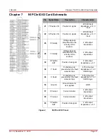
Chapter 7: NI PCIe 6363 Card Schematic
Rev A, November 11, 2016
Page 11
Chapter 7
NI PCIe 6363 Card Schematic
Figure 4
NI PCIe 6363 Pinout
Pin Signal Name
Description
Characteristics
21
Y Position IN
Position In signal
200 kΩ input
impedance, ± 10 V
input
22
X Position IN
Position In signal
200 kΩ input
impedance, ± 10 V
input
26
X Velocity
Voltage signal is
proportional to the
velocity of the
scanner
2 kΩ output
impedance
28
Y Velocity
Voltage signal is
proportional to the
velocity of the
scanner
2 kΩ output
impedance
30
X Position
OUT
Position Out signal
2 kΩ output
impedance, ± 4 V
38
Y Fault
Pulled down to
ground when the fault
detector trips
4.75 kΩ output
impedance to 12 V
CMOS logic
46
X Fault
Pulled down to
ground when the fault
detector trips
4.75 kΩ output
impedance to 12 V
CMOS logic
54
Ground
Ground return for
user signals
GND
57
X Current
Current monitor
2 kΩ output
impedance
60
Y Current
Current monitor
2 kΩ output
impedance
65
Y Position
OUT
Position Out signal
2 kΩ output
impedance, ± 4 V


